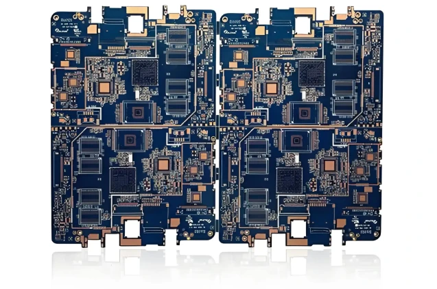
As modern electronics continue to evolve, 4-layer printed circuit boards (PCBs) have become essential across sectors like telecommunications, automotive, medical, and industrial equipment. These boards offer a reliable, compact, and high-performance foundation for increasingly complex systems that demand both signal integrity and power efficiency.
Highleap PCB Factory is a trusted manufacturer specializing in all types of PCB production and assembly, from single-layer prototypes to multilayer HDI, rigid-flex, and embedded-component boards. With advanced facilities in China and a commitment to consistent quality, rapid delivery, and competitive pricing, Highleap PCB Factory supports global engineers and procurement teams with complete end-to-end solutions.
4-Layer PCB Stackup Design: Foundation of High-Performance Circuit Boards
The foundation of a successful 4-layer PCB lies in its stackup design. In a typical configuration, two outer signal layers are combined with two inner plane layers—usually one for ground and one for power. This setup supports efficient signal routing, stable power delivery, and reduced electromagnetic interference (EMI).
An optimized stackup offers multiple benefits. It allows controlled impedance, minimizes crosstalk, and improves thermal management by strategically distributing copper. Engineers working with mixed-signal systems or high-frequency applications often adapt the standard configuration to better suit design needs. For example, placing both signal layers on top of the stack and dedicating the bottom layers to ground and power planes can improve analog/digital isolation or enhance signal integrity in high-speed designs.
In one real-world automotive project, Highleap PCB Factory helped an OEM develop a compact 0.8mm-thick 4-layer board with a tailored dielectric profile. The design achieved 50-ohm single-ended impedance with a ±5% tolerance, enabling stable performance for CAN bus communication under extreme thermal and vibration conditions.
Impedance Control in 4-Layer PCBs: Ensuring Signal Integrity for High-Speed Applications
Impedance control is one of the most critical aspects of high-speed PCB design. Whether for digital circuits, RF systems, or precision analog applications, mismatched impedance can lead to signal reflections, distortion, and poor transmission quality.
In 4-layer designs, impedance is influenced by factors such as trace width, copper thickness, dielectric constant of the materials, spacing from reference planes, and solder mask characteristics. Typical target values include 50 ohms for single-ended traces and 90 to 100 ohms for differential pairs, depending on the interface standard—such as USB 3.0, HDMI, Ethernet, or PCIe.
Advanced design techniques further ensure reliable signal integrity. These include coplanar waveguide routing for high-frequency signals, via stitching to maintain reference continuity, length matching within differential pairs, and skew control across multiple lanes. During production, Time Domain Reflectometry (TDR) is used to validate impedance characteristics on every panel, backed by pre-production simulations and impedance coupon testing.
For instance, in a 10Gbps optical module project, Highleap PCB Factory delivered boards with ±3% impedance tolerance. Through careful stackup modeling and material control, the actual measured impedance deviation was within ±2.1%, resulting in exceptional signal eye diagrams and a bit error rate below 10⁻¹².
4-Layer vs 2-Layer PCBs: Performance, Reliability, and Design Trade-offs
Choosing between a 2-layer and a 4-layer PCB design is a critical decision that affects performance, manufacturability, and long-term reliability. While 2-layer boards offer cost efficiency for basic applications, they often fall short in areas like signal integrity, EMI performance, power delivery, and thermal management.
4-layer PCBs provide significant advantages. With dedicated power and ground planes, they enable cleaner signal transmission, lower impedance power paths, and better heat dissipation. The increased routing layers also support higher component density and smaller board sizes, especially in designs that require multiple BGA packages or high-speed differential routing.
Although a 4-layer board may cost 40–60% more than a 2-layer alternative, the investment often leads to overall cost savings. Engineers can reduce the number of external components (such as EMI filters), accelerate layout cycles, and improve system stability—ultimately cutting down development time and warranty claims.
Real-world examples speak volumes. In one automotive infotainment project, the switch to a 4-layer PCB resulted in a 15 dB improvement in EMI performance and a 40% reduction in PCB area. A medical device manufacturer leveraged 4-layer technology to eliminate image noise in ultrasound systems and shrink their enclosure size by 30%. In the industrial IoT sector, a wireless gateway product improved its communication success rate from 78% to 95% after transitioning to a 4-layer design with integrated RF and cellular antennas.
Why Choose China for 4-Layer PCB Manufacturing: Quality, Cost, and Speed Combined
China continues to lead the global PCB industry by combining advanced technology, high manufacturing capacity, and exceptional cost efficiency. For companies worldwide, partnering with a trusted Chinese manufacturer like Highleap PCB Factory provides access to high-end production capabilities without compromising on quality or delivery timelines.
Chinese facilities offer a full range of capabilities including HDI processing, rigid-flex integration, buried/blind via technology, and the use of high-frequency materials such as Rogers, Isola, and Taconic. Equipment is sourced from global leaders, ensuring precision and repeatability. Certification standards include ISO 9001, IATF 16949, ISO 14001, and ISO 13485, with full compliance to RoHS, REACH, UL, and IPC Class 2/3 manufacturing criteria.
Highleap PCB Factory maintains rigorous quality control at every stage. This includes incoming material inspection, in-process monitoring, electrical testing, AOI and flying-probe inspection, as well as environmental reliability tests such as thermal cycling and humidity exposure. For critical projects, customer-specific testing and reporting are also available.
When it comes to logistics, Highleap offers flexible shipping options to meet diverse customer needs. Rapid prototyping can be delivered within 3–5 working days, small batch production in under 8 days, and volume orders within 8–15 days. For urgent schedules, 24–48 hour expedited builds are also available. Orders are shipped globally using FedEx, DHL, UPS, and consolidated freight for mid- to large-volume production.
In terms of technical capabilities, Highleap PCB Factory supports minimum trace/space widths of 3 mil, mechanical vias down to 0.1 mm, laser vias as small as 0.05 mm, and copper weights up to 6 oz. Special technologies include impedance-controlled routing with ±3% tolerance, embedded components, and advanced material stackups for high-frequency or high-reliability applications.
Ready to move forward with your 4-layer PCB project? Whether you’re developing next-generation communication equipment, automotive control units, medical electronics, or industrial automation systems, Highleap PCB Factory is ready to support your success.
Contact us now for:
- Free design-for-manufacturing (DFM) reviews
- Stackup optimization and material guidance
- Competitive quotes with clear cost breakdowns
- Fast-turn prototyping and mass production services
Let us help you bring your ideas to market—faster, better, and with complete technical confidence.