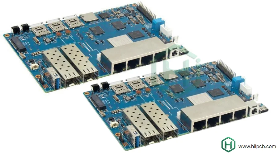
4G LTE technology is essential for mobile broadband, IoT connectivity, and mission-critical communications. Despite the rise of 5G, 4G networks will continue to expand, especially in cost-sensitive markets.
Our 4G PCB manufacturing supports equipment manufacturers deploying base stations, developing mobile devices, and creating IoT solutions that leverage LTE’s global availability, reliability, and cost-effectiveness.
What Are the Key Requirements for 4G PCBs?
4G PCBs must meet technical requirements for reliable operation across LTE’s frequency bands, while remaining cost-effective for mass-market deployment.
- Frequency Range and Bandwidth: 4G LTE operates from 450 MHz to 3.5 GHz, requiring careful impedance control and low-loss routing. FR4 PCB is often used, reducing material costs while maintaining RF performance.
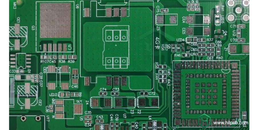
- Multi-Band and Multi-Mode Support: 4G devices support multiple frequency bands and technologies like LTE, GSM, and WCDMA. HDI PCBs are often used for mobile devices to handle complex signal routing.
- Power Efficiency: Low-power design is crucial for mobile devices. Advanced PA architectures like envelope tracking require high-efficiency PCBs to maintain signal integrity and improve battery life.
- Signal Integrity: 4G modulation schemes like 64-QAM demand clean signal paths. We ensure controlled impedance, proper termination, and power supply filtering for minimal distortion.
- Thermal Management: Power amplifiers dissipate significant heat. Metal core PCBs or high thermal PCBs are used to ensure heat dissipation and prevent component damage.
- Cost Targets: 4G technology requires cost-effective PCB manufacturing. Standard FR4 materials are used in most applications, while heavy copper is selectively employed in high-power areas to improve thermal management.
Choosing the Best Materials for 4G PCBs
Material selection impacts 4G PCB performance, thermal characteristics, reliability, and cost. We focus on finding the optimal balance between these factors.
Standard FR4 Performance: Modern FR4 materials like Isola I-Speed offer a dielectric constant of 3.7-4.3, suitable for most 4G applications at a lower cost than high-frequency laminates.
Enhanced FR4: For base stations and premium mobile devices, we use mid-loss FR4 materials with improved efficiency for power amplifiers and lower noise figures.
Rogers Materials for Optimal Performance: For the highest RF performance, Rogers PCBs such as RO4350B offer low dissipation factors and precise impedance control, reducing insertion loss.
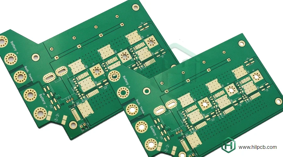
Copper Weight: Heavy copper PCBs are used for power distribution in base stations to reduce resistive losses. We use 2-10 oz copper for high-current applications and optimize copper weight for signal integrity and thermal management.
Surface Finish: ENIG provides excellent solderability and long shelf life. For lower RF loss, immersion silver is selected, especially for high-frequency applications.
How to Minimize Losses and Crosstalk in 4G PCBs
Signal quality is critical for 4G system performance. Minimizing losses and crosstalk ensures efficient communication and high data throughput.
Key strategies for minimizing losses and crosstalk include:
- Transmission Line Optimization:
Properly designed microstrip and stripline traces ensure minimal insertion loss. We calculate trace width and use smooth copper foils to reduce skin effect losses. - Via Optimization:
Minimizing via count and optimizing via geometry reduces impedance discontinuities. Multilayer PCBs with buried vias are used to eliminate stubs and minimize signal loss. - Ground Plane Design:
Solid ground planes ensure low-impedance return paths and prevent EMI. We use via stitching to connect ground planes at regular intervals to maintain signal integrity. - Isolation Techniques:
We maintain isolation between RF paths by increasing trace spacing and using ground traces for additional shielding. Guard traces and physical separation enhance isolation for sensitive signals. - Crosstalk Reduction:
Proper routing of differential pairs and maintaining spacing between traces reduce crosstalk. We simulate using field solvers to ensure minimal coupling and signal degradation. - Power Supply Noise:
We implement multi-stage filtering to isolate power supply noise from sensitive RF and analog circuits, ensuring clean signal paths and improving overall performance.
Ensuring Consistency and Reliability in 4G PCBs
Ensuring long-term reliability in 4G PCBs requires stringent quality control and thorough testing.
Key aspects of our reliability process include:
Manufacturing Process Control:
Our SMT assembly lines follow strict process controls with real-time monitoring to ensure precise placement and soldering, preventing defects.Material Qualification:
Materials are sourced from qualified suppliers, and we conduct incoming inspections to verify specifications like dielectric constant and copper weight.Design Validation:
Prototypes are validated through electrical testing and environmental stress tests to ensure they meet performance criteria before full production begins.Reliability Testing:
We conduct HALT (Highly Accelerated Life Testing), thermal cycling, and shock/vibration tests to assess long-term performance, ensuring the PCB will withstand real-world conditions.Field Failure Analysis:
In case of failures, we conduct thorough root cause analysis to prevent future issues, maintaining a high standard of quality throughout production.
Custom 4G PCBs: Pricing and Lead Time Explained
Understanding 4G PCB costs and schedules helps with effective project planning.
Key factors include:
- Prototype vs Production Costs: Prototypes involve setup expenses, while production costs are lower due to economies of scale. Volume production reduces setup costs and optimizes material procurement.
- Material Cost Drivers: FR4 materials are cost-effective, while Rogers materials and heavy copper increase costs, but offer superior performance for high-power or high-frequency applications.
- Layer Count Economics: Adding layers increases costs non-linearly. A move from 4 to 6 layers adds 40-60% to the cost, while 8-10 layers double costs.
- Complexity Factors: HDI PCBs and high-frequency designs are more expensive due to smaller traces and via structures.
- Lead Time Considerations: Standard lead time is 2-4 weeks for PCBs, with expedited services available for faster delivery. Material procurement may take longer for specialized materials like Rogers or heavy copper.
- Volume Discounts: Higher quantities lead to volume discounts, reducing costs as production volume increases.
PCB Manufacturing and Assembly for Wireless and High-Performance Devices
At HILPCB, we specialize in providing advanced PCB manufacturing and assembly solutions for a wide range of industries, including 5G, 4G, IoT, automotive, and industrial applications. Our goal is to deliver high-performance, reliable, and cost-effective PCBs tailored to your specific requirements.
Key Applications for Our PCB Solutions:
- Mobile Phones: HDI PCBs with fine-line traces and microvias for high-density, compact designs in mobile devices, ensuring reliable performance and connectivity.
- IoT Modules: Low-layer-count PCBs designed for low power consumption and compact form factors, optimized for efficient operation in IoT devices.
- Base Stations: Multilayer PCBs with heavy copper and thermal management for high-power distribution and signal routing in 4G and 5G base stations.
- Automotive Telematics: Rigid-flex PCBs for automotive applications that require flexibility, durability, and reliable connectivity in challenging environments.
- Industrial Equipment: Rugged PCBs built for harsh environments, offering enhanced protection against moisture, vibration, and thermal stress, ensuring long-term reliability.
At HILPCB, we provide tailored solutions for every stage of the PCB lifecycle—design, manufacturing, assembly, and testing—ensuring high quality and on-time delivery for all your projects.
Request your PCB quote today and leverage our expertise in PCB manufacturing and assembly to bring your ideas to life!