Effective thermal management begins with intelligent aluminum substrate design. Although aluminum substrates have superior heat dissipation compared to FR4, achieving optimal performance requires careful attention to the placement of thermal vias, copper thickness selection, component layout, and electrical isolation strategies.
Poor design decisions can negate the thermal advantages of the aluminum substrate material. Insufficient thermal via coverage creates hot spots, shortening component lifespan. Insufficient copper thickness leads to resistive heating. Improper component spacing causes thermal coupling, where heat from one device raises the ambient temperature of adjacent devices. These issues compromise reliability and waste the material cost premium.
At HILPCB, we offer design review and optimization services for aluminum substrates. Our engineering team combines Metal Core PCB expertise with thermal simulation capabilities to help customers achieve maximum performance from their designs.
Aluminum Substrate Stack-up Configurations for Optimized Thermal Management
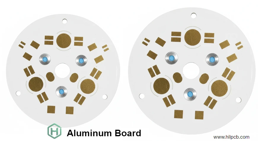
Single-Sided Aluminum Substrate Design
The most common aluminum substrate structure places all components and copper traces on one side, with the aluminum substrate on the other side. This configuration is suitable for over 80% of thermal management applications.
Advantages of Single-Sided Aluminum Substrate Design:
- Cost-Effective: Manufacturing costs are 30-50% lower than double-sided designs.
- Simplicity: Simplified design and assembly process.
- Optimal Thermal Performance: Shortest path for heat dissipation to the aluminum substrate.
- Standard Assembly: Compatible with standard SMT assembly processes.
Design Considerations:
- Single-Layer Routing: All traces must be routed on one side of the board.
- Component Density: Limited by single-sided layout.
- Trace Crossings: Require jumpers or zero-ohm resistors.
- Complexity: Complex circuit designs require careful planning.
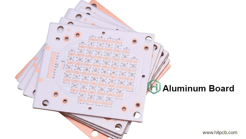
Double-Sided Aluminum Substrate Design for Higher Circuit Density
For advanced applications requiring higher circuit density, special blind via technology can be used to route traces on both sides of the aluminum substrate.
Advantages of Double-Sided Aluminum Substrate Design:
- Increased Component Density: Enables more compact designs, optimizing board space.
- Flexible Routing: Provides more design flexibility to reduce overall board size.
- Double-Sided Component Placement: Allows placement of low-power components on both sides of the board.
Challenges:
- Higher Manufacturing Costs: 60-100% more expensive than single-sided designs.
- Thermal Management Complexity: Requires careful thermal analysis to ensure effective heat dissipation.
- Limited Via Options: Only blind and buried vias are available; no through-holes.
- Specialized PCB Manufacturing: Requires advanced PCB manufacturing capabilities.
Selecting the Right Copper Thickness for Aluminum Substrate Design
Copper thickness plays a key role in both the electrical performance and thermal spreading of aluminum substrate designs:
1–2 oz Copper (Standard): Suitable for signal traces and medium-power distribution (up to 10A). This copper weight is easy to handle in standard PCB manufacturing processes, with low cost and fast lead times.
3–6 oz Copper (Heavy Copper): Necessary for high-current power distribution (10–30A) or for copper traces acting as lateral heat spreaders. This improves thermal management by reducing resistive heating and enhancing heat distribution across the aluminum substrate.
8–10 oz Copper (Extreme Heavy Copper): Required for very high currents (50A and above) or applications with demanding thermal requirements. Integration with Heavy Copper PCB technology provides electrical and thermal advantages but significantly increases cost (+40–80%) and manufacturing complexity.
For most applications, using a combination of copper thicknesses on a single board helps balance cost and performance. Heavy copper should be used only where current or thermal requirements justify it, with standard copper for signal traces.
Component Layout Strategies
Heat Source Distribution
Distribute high-power components across the entire aluminum substrate area rather than concentrating them in one region. Even with excellent aluminum substrate performance, concentrated heat sources can overwhelm local thermal capacity.
Best Practices: Maintain a minimum spacing of 10–15mm between components dissipating >2W. For components exceeding 5W, increase spacing to 15–20mm or more based on thermal simulation results.
Thermal Coupling Effect: Components placed too close together create thermal coupling, where heat from one component raises the ambient temperature of adjacent components. This叠加效应 can lead to failure, even if individual components are operating within their ratings.
Hot Spot Management
Identify areas of maximum thermal density during the layout phase. Components dissipating >10W in an area smaller than 4cm² require special attention and enhanced thermal management:
- Dense arrays of thermal vias with 0.8mm pitch or tighter
- Thick copper traces (3–6 oz) for lateral heat spreading
- Direct heat sink contact via board cutouts or openings
- Active cooling (fans, forced convection) for extreme power densities
Temperature-Sensitive Component Placement
Place precision analog components away from major heat sources to prevent temperature-induced drift:
Temperature-Sensitive Devices:
- Voltage references (drift specification ≤25ppm/°C)
- Precision resistors (temperature coefficient ≤50ppm/°C)
- Crystal oscillators (frequency stability requirements)
- Analog-to-digital converters (offset and gain temperature errors)
Layout Guidelines: Maintain a distance of >20mm from any component dissipating >5W. The efficient heat dissipation of the aluminum substrate PCB base material means thermal effects extend several centimeters from power components. Use thermal simulation to verify temperature distribution.
Copper Trace Design for Current and Thermal Management
Current Capacity Calculation
Use the IPC-2221 standard as a baseline and modify it based on the enhanced cooling of the aluminum substrate:
Standard IPC Formula: I = k × ΔT^0.44 × A^0.725
Where:
- I = Maximum current (Amperes)
- k = Material constant (0.048 for outer layers)
- ΔT = Temperature rise relative to ambient (°C)
- A = Cross-sectional area (square mils)
Aluminum PCB Modification: The aluminum substrate effectively cools the copper traces, theoretically allowing 20–30% higher current density than FR4 for the same temperature rise. However, conservative design practices recommend using standard IPC calculations with a 10–15% safety margin.
Power Distribution Design
Wide Copper Pours: Use copper pour areas instead of narrow traces for power distribution. Minimizes resistive losses (I²R heating) and provides excellent lateral heat spreading from local hot spots.
Voltage Drop Calculation: For a 10A, 12VDC scenario over a 100mm trace length, a 3mm wide, 2oz copper trace exhibits approximately 0.6Ω resistance at 20°C, resulting in 6W of dissipation and a 0.6V voltage drop. Increase to 6oz copper or wider traces for better performance.
Heavy Copper Integration: When current requirements exceed 30–50A, standard aluminum circuit board structures become inadequate. Integration with Heavy Copper PCB technology using 8–10 oz copper provides the necessary current capacity while maintaining thermal performance.
Thermal Relief Patterns
Standard thermal relief patterns used in FR4 designs can be counterproductive in aluminum substrates, where maximizing thermal connection is the priority:
For Non-Critical Pads: Use full direct connection to copper pour for maximum heat transfer For Hand-Soldered Pads: Limited thermal relief is acceptable (2–4 spokes, 0.3–0.4mm width) to reduce heat sinking effect during manual assembly For High-Power Device Pads: Always use full copper connection – thermal management takes priority over soldering convenience
HILPCB One-Stop Design and Manufacturing Services
At HILPCB, we offer comprehensive, end-to-end PCB solutions – from design to assembly, testing, and packaging. Our expertise covers all types of PCBs, including aluminum substrates, metal core PCBs, HDI boards, flexible PCBs, and more. Whether you need a simple design or an advanced high-performance PCB, we have the capability to deliver.
- Design Review: Our experienced engineers conduct a thorough review of your PCB layout, identifying thermal optimization opportunities, improving performance, and addressing potential reliability issues before production.
- Thermal Analysis: Using Finite Element Analysis (FEA) simulations, we predict component temperatures and suggest improvements to enhance thermal management. This service is available for pre-production validation and troubleshooting during production.
- Assembly and Testing: From surface mount to through-hole assembly, we offer complete PCB assembly services, ensuring your boards are ready for the field. We also provide comprehensive testing – from electrical to thermal performance validation – ensuring your PCBs meet the highest quality and reliability standards.
- DFM (Design for Manufacturability) Feedback: We optimize your design for cost-effective production. Our team reviews tolerances, materials, panelization, and manufacturing constraints to ensure your PCB is both high-quality and cost-effective.
Our PCB manufacturing facilities are well-equipped to handle every step of the process with precision and efficiency. Whether you need high-volume production or custom small-batch runs, we ensure every project receives the attention it deserves from start to finish.