Highleap PCB Factory (HILPCB) specializes in manufacturing premium aluminum nitride PCBs that deliver unmatched thermal performance for power electronics, RF amplifiers, LED modules, and laser diode applications. Our advanced AlN substrate processing capabilities, combined with precision metallization technologies, produce aluminum nitride circuit boards that excel where traditional materials fail.
Superior Thermal and Electrical Properties of AlN Substrates
Aluminum nitride represents the optimal balance of thermal conductivity, electrical insulation, and mechanical stability among ceramic PCB materials. The unique crystalline structure of AlN delivers exceptional performance characteristics:
Thermal Excellence
- Thermal conductivity: 170-230 W/m·K (5-7x better than alumina)
- Thermal expansion: 4.5 ppm/K closely matching silicon
- Maximum operating temperature: 1000°C in inert atmosphere
- Thermal shock resistance: ΔT >300°C
Electrical Properties
- Dielectric constant: 8.8 at 1 MHz with minimal frequency dependence
- Volume resistivity: >10¹⁴ Ω·cm at room temperature
- Dielectric strength: >15 kV/mm
- Loss tangent: 0.0003 at 1 GHz
These properties make aluminum nitride PCBs indispensable for applications requiring simultaneous high power handling and electrical isolation. Unlike metal core PCB solutions that require dielectric layers limiting thermal performance, AlN substrates provide direct thermal paths while maintaining complete electrical isolation.
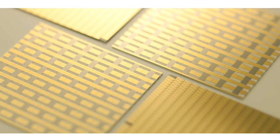
Advanced Manufacturing Processes for AlN PCB Production
Manufacturing aluminum nitride circuit boards demands specialized processes adapted to the material's unique properties:
Substrate Preparation
The AlN substrate undergoes precision lapping to achieve a surface roughness below 1 μm, critical for reliable metallization. It is then cleaned ultrasonically using specialized solvents to remove microscopic residues. To prevent surface oxidation and maintain material integrity, the substrates are stored in a controlled atmosphere. Laser scribing is employed for singulation, offering stress-free separation without mechanical damage or edge cracking.
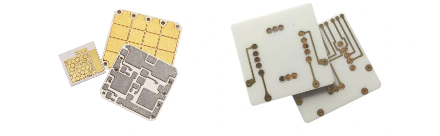
Metallization Technologies
We employ a range of metallization techniques, each matched to specific application needs:
- Thin Film Metallization utilizes titanium or titanium nitride (Ti/TiN) as adhesion layers, with gold (Au) or copper (Cu) serving as the conductive material. This method is ideal for high-frequency RF and microwave circuits requiring fine line resolution and low loss.
- Thick Film Metallization is commonly used in power electronics, using a molybdenum-manganese (Mo-Mn) adhesion system with silver (Ag) or silver-palladium (AgPd) conductors. It provides robust current handling and cost-effective production.
- Direct Bond Copper (DBC) technology relies on a copper oxide eutectic reaction to bond copper directly to the ceramic substrate. This technique is suited for high-current applications due to its excellent thermal and electrical conductivity.
- Active Metal Brazing (AMB) employs titanium or zirconium (Ti/Zr) as active elements in combination with copper or silver conductors. This process creates hermetic seals and is commonly used in aerospace and high-reliability packages.
All thin film metallization processes are carried out in Class 1000 cleanroom environments. These ultra-clean conditions are essential for ensuring contaminant-free surfaces, consistent film thickness, reliable adhesion, and optimal electrical performance—especially critical in high-frequency and high-power applications.
High-Power Applications and Thermal Management Solutions
AlN PCBs excel in dissipating heat from high-power components:
Power Electronics Integration
- IGBT and SiC MOSFET modules with integrated cooling
- Direct die attachment reducing thermal resistance by 60%
- Current handling exceeding 200A with proper copper thickness
- Junction-to-case thermal resistance <0.2 K/W
RF Power Amplifier Solutions
- GaN-on-AlN integration for maximum efficiency
- Thermal via arrays with <0.5mm pitch
- Embedded cooling channels for liquid cooling
- Power density exceeding 10W/mm² at device level
LED and Laser Diode Applications
Our aluminum nitride substrates enable:
- COB LED arrays with 200W+ power handling
- Laser diode bars with integrated micro-channel cooling
- UV LED modules with enhanced reliability
- Thermal resistance 70% lower than alumina alternatives
We provide thermal simulation services optimizing copper coverage, via placement, and component positioning for maximum heat spreading efficiency.
Complete AlN PCB Assembly and Integration Services
Beyond substrate manufacturing, HILPCB offers specialized assembly services for aluminum nitride PCBs:
Assembly Capabilities
- Die attachment using AuSn, AuGe, or sintered silver
- Wire bonding with 25-75μm Au or Al wires
- SMT assembly adapted for ceramic substrates
- Hermetic sealing for environmental protection
Process Optimization
- Controlled atmosphere soldering preventing oxidation
- Multi-zone reflow profiles accommodating AlN's thermal mass
- X-ray inspection ensuring void-free die attachment
- Pull testing validating wire bond strength
Our turnkey assembly services include component sourcing, programming, and burn-in testing, delivering complete aluminum nitride PCB solutions ready for system integration.
Why Choose HILPCB for Your AlN PCB Manufacturing
Partnering with HILPCB for aluminum nitride PCB manufacturing brings distinct advantages that accelerate your product development while ensuring exceptional quality. Our dedicated AlN processing facility combines advanced equipment with experienced engineers who understand the nuances of ceramic substrate manufacturing. From initial design consultation through volume production, we provide comprehensive support that transforms your thermal management challenges into reliable solutions.
Our commitment to excellence extends throughout the entire customer experience. Quick-turn prototyping services deliver AlN PCBs in 7-10 days, enabling rapid design iteration and validation. For production volumes, our automated handling systems and rigorous quality controls ensure consistent performance across every batch. With monthly capacity exceeding 20,000 aluminum nitride substrates and established relationships with material suppliers, we maintain the flexibility to scale with your growing requirements.
Choose HILPCB as your aluminum nitride PCB partner and benefit from our technical expertise, manufacturing excellence, and unwavering commitment to customer success. Whether you're developing next-generation power modules, RF amplifiers, or high-brightness LED systems, our AlN solutions provide the thermal performance and reliability your applications demand. Contact us today to discuss how our aluminum nitride PCB capabilities can enhance your product's performance and accelerate your time to market.
FAQ
What makes aluminum nitride superior to other ceramic materials?
AlN offers the best combination of high thermal conductivity (170-230 W/m·K) and electrical insulation among non-toxic ceramics. Its thermal expansion closely matches silicon devices, reducing stress during thermal cycling. Compared to alumina, AlN provides 5-7x better thermal performance while maintaining excellent electrical properties.
How do AlN PCB costs compare to traditional solutions?
Aluminum nitride substrates cost 5-15x more than FR-4 but often reduce total system cost by eliminating heatsinks, improving reliability, and enabling higher power density. For applications requiring >10W heat dissipation, AlN often provides the lowest cost per watt of thermal management.
What are typical lead times for aluminum nitride PCB orders?
Standard AlN PCB designs ship in 10-15 days, with expedited 7-day service available for prototypes. Complex assemblies with die attachment and wire bonding typically require 15-20 days. We stock common AlN substrate sizes to minimize material procurement delays.
Can aluminum nitride be used for RF and microwave applications?
Yes, AlN excels in high-frequency PCB applications with low dielectric loss (tan δ < 0.001) and stable dielectric constant. The material supports frequencies exceeding 40 GHz with proper metallization. Many RF power amplifier designs utilize AlN for simultaneous thermal management and impedance matching.
What design considerations are unique to AlN PCBs?
Design rules include minimum trace width of 100μm, via diameter of 100μm, and edge clearance of 0.5mm to prevent chipping. Thermal vias should be arrayed with <2mm spacing for effective heat spreading. We provide comprehensive design guidelines and review services to ensure manufacturability.
How do you ensure quality and reliability of AlN PCBs?
Our quality system includes incoming material inspection, in-process monitoring, and final testing per IPC and MIL standards. We perform adhesion testing, thermal cycling, and moisture resistance validation. All products include material certificates and test reports documenting compliance with specifications.