Ceramic circuit boards are ideal for high-frequency, high-voltage, or heat-intensive environments. At Highleap PCB Factory, we specialize in building custom ceramic PCBs using alumina, aluminum nitride, and other engineered ceramics that combine strength, electrical insulation, and outstanding thermal conductivity.
From RF modules and power amplifiers to high-density LED platforms and aerospace-grade modules, we support design teams with fast lead times and precise builds.
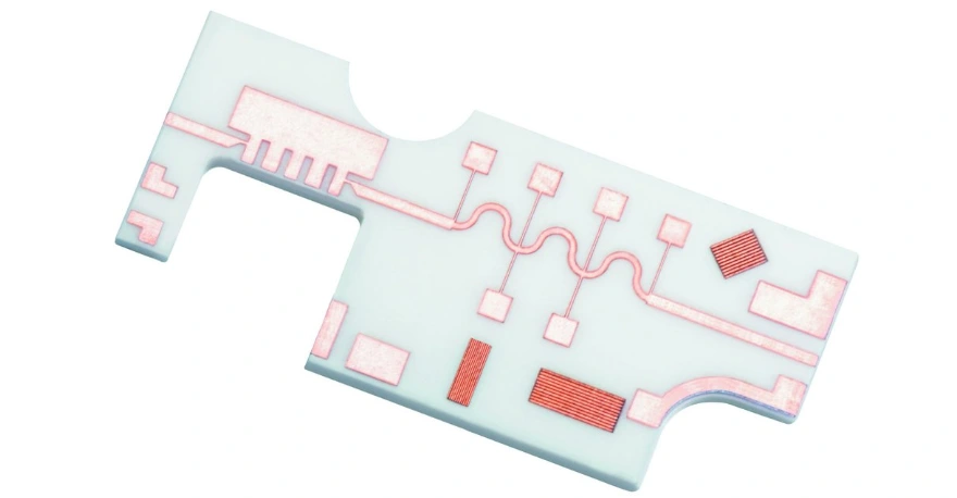
Explore our product categories or learn more about our PCB manufacturing capabilities.
Ceramic PCB Configurations and Material Pairings
To support diverse design needs, we offer a range of material and layout choices:
| Material Type | Use Case | Notes |
|---|---|---|
| Alumina (Al2O3) | LED, RF, control | Cost-effective, reliable |
| Aluminum Nitride (AlN) | High-power, thermal | Superior conductivity |
| Zirconia | Sensor platforms | Tough and chemically stable |
| Metallization | AgPd, Au, Cu | For direct bonding and wire bonding |
| Finish Options | ENIG, OSP, Ag | Compatible with gold wire bonding |
We also support multilayer ceramic circuit board builds using LTCC or thick-film hybrid technology for special applications.
Design Considerations for Ceramic Circuit Boards
Working with ceramic circuit board technology requires specialized layout and production understanding. Unlike FR4-based boards, ceramic PCBs have unique physical and thermal behaviors that directly impact manufacturability and performance. At Highleap, we help engineering teams adapt their existing stack-ups and routing to suit the properties of ceramic substrates.
Ceramic boards are dimensionally stable and support high-frequency signals, but they are more brittle and must be handled differently during both drilling and assembly. Standard mechanical vias may be replaced with laser-formed structures. Conductive layers are often screen-printed or plated with silver-palladium or gold systems for better bonding and conductivity.
Additionally, ceramic substrates enable direct heat transfer from components to enclosures or heatsinks. This thermal efficiency makes them ideal for high-power LED systems, RF amplifiers, and embedded control modules. Our engineering team often recommends design strategies such as split ground planes, isolated thermal islands, or silver-filled thermal vias to optimize heat distribution.
For designers shifting from standard PCB materials to ceramic, we provide guidance on layout constraints, edge clearance, metallization compatibility, and packaging options. Our full PCB manufacturing process is equipped to handle both thin-film and thick-film ceramic production technologies with advanced lamination and metallization control.
For designers unfamiliar with ceramic PCB fabrication, here’s how layout rules differ:
| Area | Ceramic Boards | Standard FR4 |
|---|---|---|
| Vias | Laser-drilled or punched | Mechanically drilled |
| Conductors | Screen-printed or plated | Etched copper foils |
| Tolerances | Tighter dimensional control | More lenient |
| Mounting | Direct die attach and silver epoxy | Solder paste with FR4 pads |
| Fragility | Brittle substrate | Fiberglass base |
Understanding these differences helps ensure first-pass success when transitioning from FR4 to ceramic circuit board designs.
Full-Service Ceramic Circuit Board Manufacturer and Assembler
Highleap supports the complete ceramic PCB process:
- File check and layout adaptation for ceramic constraints
- Substrate sourcing (AlN, Al2O3, BeO optional on request)
- Screen printing, sintering, and metallization
- SMT and die-attach using conductive pastes or epoxy
- AOI, X-ray inspection, and test fixture design
- Global logistics with protective packaging and flexible payment options
Try our Gerber Viewer or 3D Viewer to verify design integrity before submission.
Conclusion
As a trusted ceramic circuit board manufacturer and assembly partner, Highleap PCB Factory is ready to support your most demanding projects. Whether you're building RF modules, high-voltage power delivery boards, or dense LED arrays, we have the tools, expertise, and materials to deliver precision results at speed.
Our services are built for professionals who value fast turnaround, stable quality, technical clarity, and global fulfillment. We handle difficult stack-ups, sensitive metallization, and thermal-sensitive packages with full in-house control.
From prototype to full production, we help you move forward—quickly and confidently—with ceramic PCB solutions engineered to perform. We collaborate with developers across industries—RF communications, laser driver systems, and aerospace modules—to deliver stable, repeatable results with each order.