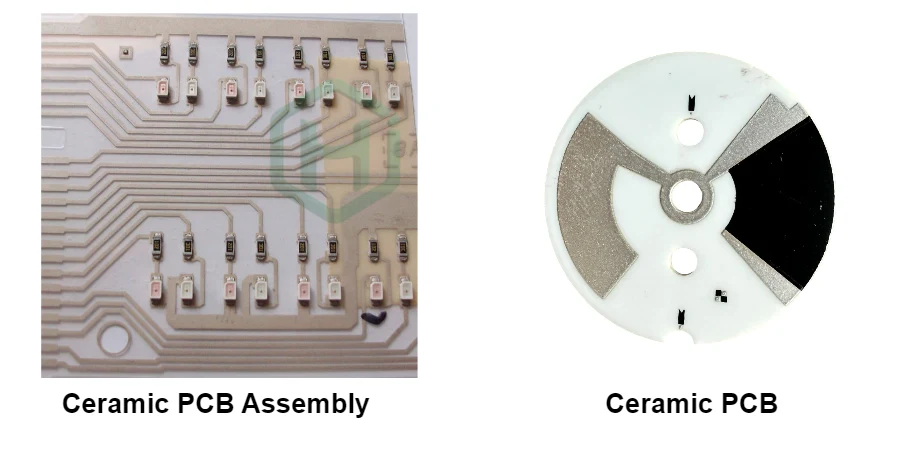
Standard assembly processes fail where performance is paramount. For high-power, high-frequency systems that operate in extreme environments, ceramic PCB assembly is the key to achieving the necessary precision, thermal reliability, and long-term stability.
At HILPCB, we are specialists in this demanding field. We provide a vertically integrated solution—from initial ceramic PCB manufacturing to final assembly, functional testing, and packaging. This turnkey approach delivers the consistent, mission-critical quality required for advanced automotive, aerospace, and medical electronics.
Why Ceramic PCB Assembly Requires Specialized Expertise
Assembling components on ceramic substrates like Alumina (Al₂O₃), Aluminum Nitride (AlN), and Silicon Nitride (Si₃N₄) is fundamentally different from working with standard FR-4. The unique material properties of ceramics present challenges that demand specialized equipment, materials, and process control.
- High Thermal Mass: Ceramics absorb and hold significantly more heat than FR-4. This requires a carefully controlled and longer reflow profile to achieve proper solder joint formation without damaging components.
- Coefficient of Thermal Expansion (CTE): While the low CTE of ceramics is an advantage for matching with semiconductor dies, a mismatch with large components can induce mechanical stress during thermal cycling if not managed correctly.
- Surface Properties: The smooth, non-porous surface of ceramic can affect solder paste adhesion and wetting if the printing process is not perfectly optimized.
Mastering these challenges is the difference between a functional prototype and a product that will operate reliably for years.
Mastering the Challenges of SMT Assembly on Ceramic Substrates
The most critical stage of ceramic PCB assembly is the Surface Mount Technology (SMT) process. Every step, from solder paste printing to reflow, must be precisely calibrated to the unique thermal and physical properties of the ceramic substrate.
The Solder Paste Printing Challenge
Achieving a perfect solder paste deposit is the foundation of a reliable solder joint. On rigid ceramic surfaces, this requires advanced control.
- Solder Paste Selection: We utilize high-activity, no-clean solder pastes with specialized flux chemistry engineered to promote excellent wetting on common ceramic finishes like ENIG, ENEPIG, and immersion silver. For power modules, high-lead (e.g., Pb92.5) or specialized high-temperature SAC alloys are used.
- Stencil and Printing Optimization: We use laser-cut stainless steel stencils, often with nano-coatings, to ensure clean paste release. Squeegee pressure, print speed, and separation distance are meticulously calibrated for each board. 2D/3D automated paste inspection (SPI) verifies the volume and alignment of every deposit before a single component is placed.
Precision Component Placement
Ceramic boards often feature fine-pitch components or bare dies that demand high-accuracy placement. Our SMT lines are equipped with high-resolution vision systems that can recognize fiducial marks directly on the ceramic or metallization layer. We can achieve placement accuracy down to ±25 µm, ensuring perfect alignment for BGAs, QFNs, and other complex packages.
The Critical Reflow Soldering Process
This is where expertise truly matters. An incorrect thermal profile can cause thermal shock (cracking the substrate) or poor solder joints.
- Advanced Thermal Profiling: We use multi-zone convection reflow ovens (up to 12 zones) to create a precise thermal profile. This allows for a gradual pre-heating ramp-up, a stable soak zone to activate the flux, and a controlled peak temperature before a carefully managed cool-down phase. Profiles are specifically developed for Alumina vs. AlN, which have vastly different thermal conductivities.
- Void-Free Vacuum Reflow: For high-power applications like IGBT modules or high-brightness LEDs, minimizing voids in the solder joint is critical for thermal transfer. Our vacuum reflow soldering capability removes trapped gases from the molten solder, reducing voiding to less than 1%. This ensures the lowest possible thermal resistance and maximum device reliability.
| Technique | Standard Reflow | Vacuum Reflow |
|---|---|---|
| Primary Goal | Create reliable solder joints | Eliminate solder voids |
| Void Percentage | 5-15% (Typical) | <1% (Achievable) |
| Best For | General SMT, RF circuits | High-power semiconductors, LEDs |
| Key Benefit | Cost-effective, high-throughput | Maximum thermal conductivity |
Advanced Bonding and Hybrid Assembly Techniques
Beyond standard SMT, many ceramic assemblies require chip-level or hybrid integration. HILPCB is equipped with advanced capabilities for these complex products.
- Silver Sintering: For maximum thermal performance, this pressure-assisted process creates a bond layer with thermal conductivity far superior to any solder, ideal for power semiconductor dies.
- Epoxy Die Attach: Electrically conductive or non-conductive epoxies are used for attaching sensitive optical components or RF dies where precise alignment is critical.
- Wire Bonding (Au/Al): We perform automated wedge and ball bonding to create interconnects on HTCC PCB and hybrid Thin Film PCB packages.
Uncompromising Quality Assurance for Zero-Defect Assembly
In high-reliability applications, there is no margin for error. HILPCB's multi-stage inspection and testing protocol ensures that every assembly meets the highest standards of quality and performance.
- Automated Optical Inspection (AOI): Post-reflow inspection to detect component misalignment, solder bridges, and wetting issues.
- X-ray Inspection (2D & 3D): Essential for verifying the integrity of solder joints hidden beneath packages like BGAs and QFNs, specifically checking for voids and shorts.
- In-Circuit Testing (ICT) & Flying Probe: Verifies electrical connectivity, component values, and polarity.
- Thermal Cycling & Burn-In: The assembly is subjected to environmental stress testing to expose any latent defects and validate long-term reliability.
- Functional Testing: Final confirmation that the assembly performs to its specified electrical parameters.
All our processes conform to the rigorous IPC-A-610 Class 3 standard, ensuring reliability for the most demanding aerospace, medical, and industrial systems.
Your End-to-End Partner for High-Reliability Ceramic Assembly
Choosing HILPCB means securing a partner who understands the complete lifecycle of your product. We eliminate the risks of working with multiple vendors by providing a seamless, expert-driven solution under one roof.
- One-Stop Manufacturing Solution: We take your design from bare Ceramic PCB Manufacturing to fully tested and packaged assemblies, streamlining your supply chain and accelerating time-to-market.
- Collaborative DFM/DFA Expertise: Our engineers work with you to optimize your design for manufacturability and assembly, preventing costly redesigns and ensuring the highest possible yield.
- Certified for Your Industry: With AS9100, ISO 13485, and IATF 16949 certifications, we deliver the process control and traceability that mission-critical applications demand.
- Advanced Technology for Advanced Products: From void-free vacuum reflow to silver sintering, we invest in the technology needed to build next-generation power and RF electronics.
Don't let assembly challenges limit your product's potential. Partner with HILPCB to build ceramic-based electronics with the precision, reliability, and performance to succeed in any environment.
Explore our full portfolio on the Ceramic PCB Product Page.