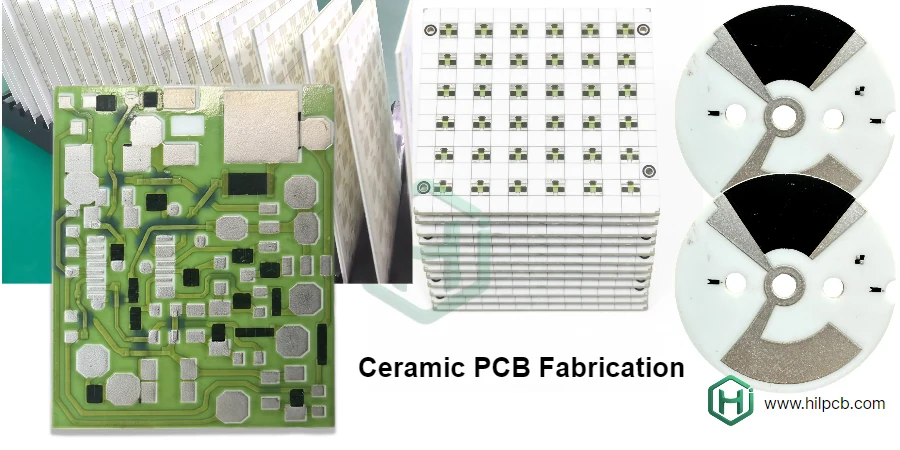
Ceramic PCB fabrication is where material science converges with precision engineering, transforming raw ceramic wafers into the high-performance heart of modern electronics. At HILPCB, we have mastered this intricate process. Our fabrication of Al₂O₃, AlN, and Si₃N₄ substrates using advanced technologies delivers the unmatched thermal conductivity and electrical insulation required for demanding power, RF, and medical applications.
Our state-of-the-art facilities integrate cleanroom manufacturing, laser machining, and automated inspection to ensure every circuit we produce meets the most stringent dimensional and electrical tolerances.
Stage 1: The Foundation – Preparing the Ceramic Substrate
Every high-reliability circuit begins with a perfect foundation. The fabrication journey starts with the meticulous preparation of high-purity ceramic wafers. This stage is critical, as it directly impacts the adhesion of the metal layers and the final dimensional accuracy of the board.
The process involves several key steps:
- Sourcing and Inspection: We begin with high-grade ceramic wafers, verifying their purity and ensuring a surface roughness of less than Ra 0.2 µm for stable dielectric performance.
- Precision Cleaning: A multi-step cleaning regimen using ultrasonic deionized water baths and chemical degreasing removes all microscopic particulates and organic contaminants.
- Surface Activation: Before metallization, a plasma activation step modifies the ceramic's surface energy, creating a highly receptive interface for the strongest possible metal bond.
Stage 2: Building the Circuitry – Metallization and Conductor Formation
This is the core stage where the electrical pathways are formed. The choice of metallization technique is dictated by the application's requirements for power handling, signal frequency, and precision.
- For High Power (DBC): In Direct Bonded Copper, thick copper foil is fused directly to the ceramic at over 1000°C, creating a robust, adhesive-free bond. This is the ideal method for power semiconductors and EV inverters that demand maximum thermal transfer and high current capacity.
- For High Precision (DPC): Direct Plated Copper fabrication is a thin-film process that uses sputtering and electrolytic plating. It allows for extremely fine lines (down to 20 µm), making it perfect for RF, microwave, and Thin Film PCB applications.
- For Extreme Durability (HTCC): In HTCC PCB fabrication, refractory metal pastes like tungsten are printed onto unfired ceramic layers and co-fired at over 1600°C. This creates a monolithic, hermetically sealed structure ideal for aerospace and implantable medical devices.
Stage 3: Defining the Details – Precision Patterning and Etching (In-Depth Focus)
If metallization lays the conductive "pavement," then patterning and etching is the art of "carving" the precise circuit design into that pavement. This stage translates the digital blueprint into a physical reality, and its accuracy directly dictates the circuit's final performance, especially in high-frequency and high-density applications.
Photolithography: Projecting the Blueprint
Performed in a cleanroom environment, photolithography is a micron-level process for transferring the circuit pattern from a photomask to the metallized ceramic substrate.
- Photoresist Application: A light-sensitive polymer, or photoresist, is uniformly applied to the metal surface via spin-coating. The uniformity of this coating is paramount for the precision of the final features.
- Exposure: A quartz photomask, which contains an opaque pattern of the circuit, is precisely aligned with the substrate. The assembly is then exposed to collimated UV light. The light passes through the clear areas of the mask, causing a chemical change in the photoresist below.
- Development: The substrate is immersed in a developer solution. Depending on the type of resist used (positive or negative), either the exposed or unexposed areas are washed away, revealing the underlying metal that is slated for etching.
Etching: Making the Pattern Permanent
Once the pattern is defined by the photoresist, etching permanently removes the unwanted metal.
- Wet Etching: The most common method, this involves immersing the substrate in a chemical bath that dissolves the unprotected metal. It is fast and cost-effective. However, its primary drawback is its isotropic nature—it etches in all directions, which can cause "undercutting" beneath the photoresist and limit the minimum achievable line width.
- Dry Etching (Ion Beam Milling): For applications demanding ultimate precision, such as microwave circuits, we use dry etching. This technique employs a focused beam of ions to physically bombard and remove the exposed metal atoms. It is an anisotropic process, creating sharp, vertical sidewalls that are critical for minimizing signal loss and achieving ultra-fine features.
| Etching Method | Principle | Advantages | Disadvantages |
|---|---|---|---|
| Wet Etching | Chemical Dissolution | Fast, Cost-Effective | Undercutting, Limited Precision |
| Dry Etching | Physical Ion Bombardment | Extremely High Precision, Sharp Edges | Slower, Higher Cost |
After etching, the remaining photoresist is stripped away, leaving a perfectly defined, high-precision circuit pattern on the ceramic substrate.
Stage 4: Vertical Interconnects – The Art of Laser Drilling and Via Plating
If metal traces are the "roads," vias are the vital "bridges" connecting different layers. Creating these in hard ceramic requires a precision that only advanced lasers can provide. Our UV and CO₂ laser systems achieve positional accuracy of ±5 µm and create holes as small as 50 µm without inducing microcracks. Following drilling, a meticulous plating process builds a uniform, reliable copper barrel within the via, ensuring a perfect electrical connection between layers.
Stage 5: The Finishing Touches – Surface Finishes and Final Machining
The final fabrication stages prepare the board for the Ceramic PCB Assembly process and ensure it meets exact mechanical specifications.
- Surface Finishing: We apply finishes like ENIG (Electroless Nickel Immersion Gold), ENEPIG, or Immersion Silver to protect the copper and provide a superior surface for soldering or wire bonding.
- Precision Machining: Using laser dicing and CNC machining, we achieve tight dimensional tolerances, ensure flatness within ±0.05 mm for die attachment, and create custom outlines or cavities. All dimensions are verified with non-contact optical metrology systems.
The HILPCB Partnership: From Concept to Component
Choosing a fabrication partner is about more than capabilities; it's about trust and collaboration. HILPCB provides a seamless, vertically integrated experience that de-risks your project and accelerates your time-to-market.
- Vertically Integrated for Unmatched Quality Control: We manage every critical step—from raw substrate preparation to final testing—under one roof. This eliminates supply chain complexity and ensures accountability and quality at every stage.
- Collaborative Engineering to De-Risk Your Design: Our DFM engineers work with you from the outset to optimize your design for manufacturability. This collaborative approach prevents costly redesigns and ensures your concept is translated into a reliable, high-yield product.
- Certified for Mission-Critical Applications: With ISO 9001, IATF 16949, and AS9100 certifications, we deliver the rigorous process control and traceability demanded by the automotive, medical, and aerospace industries.
From EV inverters and 5G base stations to medical diagnostic tools, HILPCB has the expertise to bring your most challenging ceramic PCB designs to life.
Learn more in our Ceramic PCB Manufacturing guide or explore our Ceramic PCB Product Page for detailed specifications.