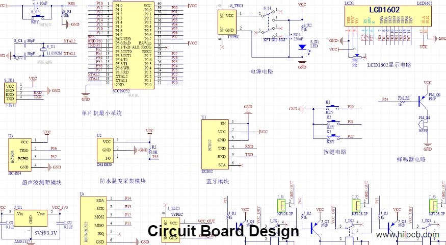
Every reliable PCB starts with a smart design. At HILPCB, our engineering team bridges the gap between concept and production by integrating Design for Manufacturability (DFM) principles from the very first schematic. This collaboration ensures your board is not only functional but also optimized for cost, quality, and yield when it enters circuit board fabrication and circuit board assembly.
1. The Importance of Design for Manufacturability (DFM)
Most PCB production issues don’t happen in the factory — they start in the design stage. Our DFM-first approach eliminates hidden risks before fabrication begins.
a) Early Collaboration Between Design and Production
We involve our manufacturing engineers as soon as the design files are received. They review stack-up compatibility, trace spacing, and via structures to ensure the layout aligns perfectly with circuit board manufacturing tolerances.
b) Design Rule Optimization
Using our internal DFM library, we adjust key parameters:
- Minimum trace/space
- Drill-to-copper clearances
- Impedance control routing
- Solder mask and stencil tolerances
This proactive alignment reduces prototype iterations and shortens your time-to-market by up to 30%.
c) Cost and Yield Optimization
We don’t just check for errors — we design for efficiency. By standardizing hole sizes, material types, and stack-up configurations, we simplify production setup and lower costs without compromising performance.
2. Signal and Power Integrity for Modern Designs
Today’s electronics operate at high speeds and low voltages — meaning signal integrity is critical. HILPCB employs advanced simulation tools to model transmission lines and power planes up to 40 GHz, ensuring predictable signal flow and minimal EMI/EMC issues.
Our design team works closely with customers in telecom, AI, and automotive sectors to build boards with:
- Controlled impedance routing
- Proper decoupling and ground referencing
- Crosstalk and reflection analysis
- Differential pair optimization
The result is a design that performs consistently from prototype through full circuit board production.
3. Circuit Board Design for Thermal and Mechanical Reliability
Effective Circuit Board Design goes beyond schematics—it must anticipate real-world operating conditions. At HILPCB, our engineers integrate thermal and mechanical reliability into every design phase, ensuring that what you design can also be built, assembled, and perform reliably.
We optimize copper thickness, layer stack-up, and via placement to balance signal integrity, heat dissipation, and manufacturability. For high-power or automotive applications, thermal simulation and mechanical stress modeling are verified directly in our in-house circuit board factory using controlled testing chambers. The result: circuit boards that are not only well-designed but also production-ready and built to last.
4. The Tools and Workflow That Keep Teams in Sync
We design using industry-standard CAD software including Altium Designer, Cadence Allegro, and Mentor Xpedition. Each file undergoes multi-step verification between design and production engineers before approval.
Our collaborative workflow includes:
- Version-controlled file management
- Automated Gerber and drill validation
- Layer stack-up documentation for traceability
- Fabrication-ready deliverables for circuit board prototyping
This integrated process prevents “design-to-fab” mismatches that often cause costly rework.
5. Why HILPCB’s Circuit Board Design Approach Works
At HILPCB, circuit board design isn’t just about schematics — it’s about creating manufacturable, high-performance boards ready for real-world production. Our integrated workflow connects design, PCB fabrication, and assembly under one roof, ensuring a smooth transition from prototype to volume manufacturing.
- End-to-end integration: Circuit board design, production, and PCB assembly managed in-house for maximum efficiency.
- Design-for-Manufacturing expertise: Early engineering feedback eliminates costly re-spins and shortens lead time.
- Global reliability compliance: IPC Class 2 & 3, ISO, IATF, and UL certified for consistent quality and traceability.
- Cross-industry experience: Proven in 5G, medical, EV, and industrial control electronics.
- Rapid production readiness: Verified design files can move to manufacturing in as little as 24 hours.
We don’t just offer Circuit Board Design — we deliver a complete design-to-production solution, built for quality, scalability, and performance.
FAQ About Circuit Board Design
1. What is Circuit Board Design? Circuit Board Design is the process of creating the layout and structure of a printed circuit board (PCB), connecting electronic components through copper traces and vias. A well-designed board improves performance, reliability, and manufacturability.
2. Which software is best for Circuit Board Design? Popular tools include Altium Designer, KiCad, Eagle, and OrCAD. The best choice depends on your project complexity, design collaboration needs, and output format for PCB fabrication.
3. How can I make my Circuit Board Design easier to manufacture? Follow Design for Manufacturing (DFM) principles—use standard footprints, adequate trace spacing, clear test points, and simple layer stackups. Working with a manufacturer early ensures your design is production-ready.
4. How much does Circuit Board Design cost? The cost depends on board complexity, layer count, design time, and simulation requirements. Basic layouts are affordable, while high-speed or RF designs require specialized engineering time.
5. What are key considerations in High-Speed Circuit Board Design? High-speed PCB design requires controlled impedance, short signal paths, and proper ground return. Designers use simulations and backdrill techniques to minimize signal loss and reflections.
6. How can I find reliable Circuit Board Design and Assembly services? Look for companies that offer both circuit board design and assembly, with IPC/ISO certifications, in-house fabrication, and proven experience in high-density, high-speed applications.