Every great product starts with a reliable printed circuit board. At HILPCB, we focus on what really matters to engineers and OEM buyers — consistent quality, predictable lead time, and direct communication with the factory that actually builds your boards.
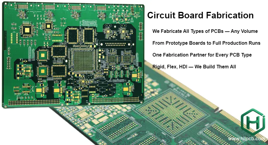
Our fabrication facility produces everything from simple two-layer PCBs to 64-layer HDI stack-ups for 5G, automotive, and AI systems — built under strict ISO and IATF standards.
1. From Design to Production-Ready Boards
Circuit board fabrication transforms your design into a high-performance structure that can survive assembly, reflow, and field operation. At HILPCB, every project starts with a Design for Manufacturability (DFM) review within hours of file submission. We check for trace spacing, impedance rules, and layer stack alignment before fabrication begins — saving time and avoiding costly redesigns.
For complex products, our engineering team coordinates directly with layout specialists to align design and manufacturing requirements, ensuring your circuit board design translates perfectly into production.
2. Material and Layer Stack Engineering
Choosing the right material is critical to balancing cost, performance, and reliability. We stock a full range of laminates, including:
- FR4 for standard commercial applications
- Rogers and Taconic for high-frequency systems
- Megtron for ultra-low-loss and high-speed networks
- Polyimide for high-temperature or flexible PCBs
For projects involving mixed signal or RF systems, our material experts fine-tune dielectric properties to maintain impedance stability and low insertion loss. This attention to stack-up detail is what makes our boards ready for volume circuit board production.
3. Step-by-Step Fabrication You Can Trust
Our fabrication process combines automation, quality control, and human expertise:
- Inner Layer Imaging – Laser Direct Imaging (LDI) ensures ±0.5 mil precision.
- Etching and Lamination – Controlled processes achieve uniform copper thickness and tight layer registration.
- Drilling and Plating – CNC and laser microvias create accurate interconnects for HDI designs.
- Solder Mask and Silkscreen – Applied under cleanroom conditions for excellent solderability.
- Electrical Testing and Inspection – 100% of boards tested before shipment.
This process consistency is why global clients trust HILPCB as their long-term fabrication partner.
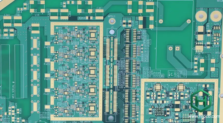
4. High-Density and Multilayer Capabilities
Modern electronics demand density without sacrificing stability. HILPCB supports:
- 2/2 mil line and space resolution
- Sequential lamination and stacked vias
- Resin-filled and capped microvias
- Impedance-controlled routing with TDR verification
We routinely deliver 32+ layer HDI boards for advanced computing, radar, and high-speed communication devices — the kind of fabrication that most general PCB vendors can’t handle.
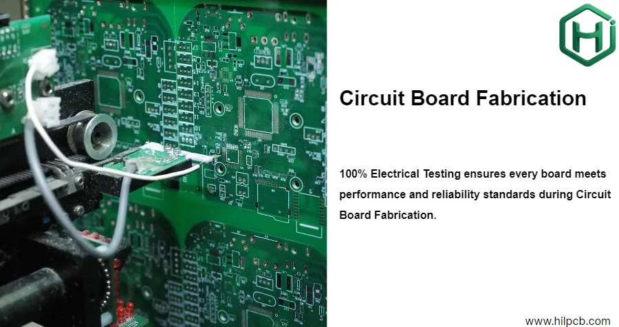
5. Precision and Reliability Through Testing
Every board we build undergoes multiple verification layers to ensure durability, conductivity, and long-term performance.
Our quality system includes:
- AOI at every imaging and etching step
- Cross-section and microvia wall analysis
- Thermal stress and peel strength testing
- Impedance and continuity validation
All results are fully traceable — ensuring reliability for your next circuit board assembly or product integration phase.
6. Avoiding the Common Pitfalls of PCB Fabrication
We understand the challenges engineers face when outsourcing fabrication — warped panels, inconsistent plating, or poor via capture. Our solution: real-time statistical process control, backed by digital feedback at every production step.
By monitoring etch rates, lamination pressure, and copper thickness in real time, we prevent defects before they happen. That’s how our circuit board factory maintains sub-1% defect rates even on complex HDI builds.
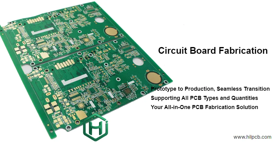
7. From Prototype to Full Production
No need to change suppliers as your product scales. HILPCB manages the entire transition — from single prototypes to mass production — using identical tooling, materials, and process profiles.
You can start with a quick-turn prototype, validated by our circuit board prototyping team, then move directly into production without requalification or data loss. This one-flow system saves weeks in product development time and ensures consistent electrical performance across all batches.
8. Why OEMs and Startups Choose HILPCB
- In-house fabrication — not a broker network
- 10+ years serving clients in 30+ countries
- Transparent communication and engineering support
- Strict quality documentation for every project
- Competitive pricing with consistent results
We’re not just another supplier; we’re a partner you can build a production plan around. That’s what makes us a trusted circuit board manufacturer for companies that can’t afford failure.
FAQ
What’s the difference between fabrication and manufacturing?
Fabrication builds the bare PCB structure. Manufacturing covers the full process — fabrication, assembly, and final testing.
Can HILPCB handle HDI and high-frequency boards?
Yes. We fabricate boards using Rogers, Taconic, and Megtron materials up to 77GHz applications.
Do you offer fast turnaround?
Yes. Standard lead time is 7–10 days; prototypes as fast as 3–5 days depending on complexity.
Can I include assembly and testing in one order?
Absolutely. We provide full turnkey production, including component sourcing and functional testing.
To learn how we extend fabrication into complete product builds, explore our full-service circuit board company overview.