In today’s compact electronic devices, the balance between routing complexity, mechanical flexibility, and durability is more critical than ever. Double layer flex PCBs provide an ideal middle ground between simple single-layer flex and expensive multilayer constructions. At HILPCB, we apply advanced flexible PCB manufacturing and assembly technologies to deliver reliable double-sided circuits that support high-speed signals, compact packaging, and long-term mechanical endurance.
Our engineering and manufacturing capabilities cover the full spectrum of flexible PCB solutions—from single layer flex PCB to rigid-flex PCB—ensuring performance, precision, and scalability across applications in automotive, consumer electronics, and medical devices.
Double Layer Flex PCB Structure and Key Benefits
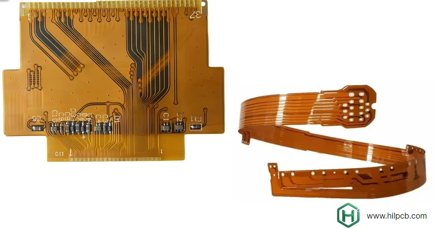
A double layer flex PCB consists of two copper layers separated by a flexible dielectric, connected through plated vias. This design doubles routing density while maintaining flexibility—ideal for curved and folded electronic assemblies. Compared to multilayer PCB constructions, it offers higher reliability under dynamic stress and lower cost for moderate signal complexity.
Key performance advantages include:
- Enhanced routing capability eliminating crossovers and jumper wires
- Dedicated ground planes improving EMI shielding and signal integrity
- Compact circuit layouts reducing connector count and form factor
- Balanced layer stack-up for uniform flexibility and mechanical stability
These benefits make two-layer flexible circuits suitable for space-constrained applications requiring reliable, repeated bending and consistent electrical performance.
Advanced Manufacturing and Quality Control
Our double layer flexible PCB manufacturing integrates precision photolithography, optical registration, and controlled impedance routing. High-resolution laser drilling enables via diameters as small as 100 μm, while advanced plating processes ensure uniform copper thickness and strong interlayer bonding.
We support both adhesive-based and adhesiveless constructions. Adhesiveless laminates deliver thinner profiles and better flexibility for compact assemblies, while adhesive-based builds provide cost-effective reliability. Symmetric dielectric structures minimize warpage during thermal cycling and reflow assembly.
Quality control spans every stage—from material verification and layer alignment to automated optical inspection (AOI) and electrical continuity testing. Environmental and mechanical validation includes flex-cycle endurance, temperature-humidity exposure, and peel-strength testing per IPC-6013 Class 3 standards.
Each project follows full traceability with documentation suitable for automotive (IATF 16949), medical (ISO 13485), and consumer electronics applications.
Applications Across Industries
Double-layer flex PCBs are widely used across industries that demand compact design, consistent performance, and mechanical flexibility.
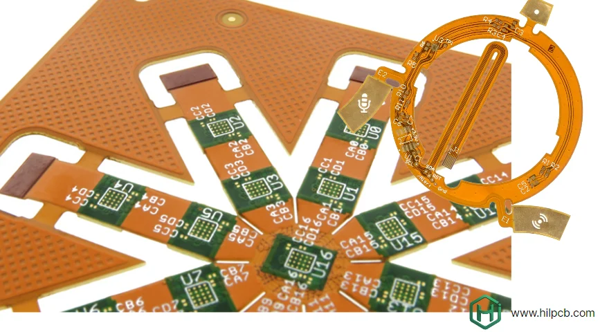
- Consumer Electronics: Used in smartphone camera modules, foldable or wearable devices, battery interconnects, and flexible display assemblies.
- Automotive Systems: Applied in ADAS sensors, infotainment units, electric vehicle battery packs, LED lighting, and curved dashboard interfaces.
- Medical Equipment: Found in diagnostic imaging systems, patient monitoring devices, implantable modules, and sterilizable flexible circuits.
- Industrial Automation: Utilized in robotic arms, motion control systems, and sensor arrays requiring dynamic movement or vibration resistance.
- Aerospace & Defense: Integrated into avionics, satellite communication modules, and lightweight control systems where space and reliability are critical.
- Telecommunication & IoT Devices: Used for antenna connections, flexible RF circuits, and compact communication modules.
Combining controlled impedance, fine-pitch routing, and long-term flex endurance, double-layer flex PCBs deliver exceptional electrical stability and mechanical reliability in environments subject to repeated bending, vibration, or thermal cycling.
Design and Assembly Considerations
Effective double layer flex PCB design minimizes stress while maintaining electrical performance. Avoid vias and heavy copper in bending areas, use rolled annealed copper for dynamic flexing, and maintain bend radii of at least 10× total thickness for long-term durability.
Our flexible PCB assembly process supports double-sided SMT placement, fine-pitch BGAs, and stiffener integration for mechanical reinforcement. Precision fixturing and optimized reflow profiles ensure flatness and solder joint integrity.
Connector design supports ZIF and board-to-board connections, with gold-plated pads for high mating cycles. Assembly inspection includes X-ray validation and functional testing for every lot.
Why HILPCB for Double Layer Flex PCB Projects
HILPCB provides end-to-end support covering design consultation, fabrication, and turnkey assembly. Our vertically integrated production combines reliability, speed, and scalability across all PCB technologies—rigid, flex, and rigid-flex.
- Proven expertise in high-density flexible PCB design and manufacturing
- Large-format and roll-to-roll production capabilities
- Certified quality systems (ISO 9001, ISO 13485, IATF 16949)
- Quick-turn prototyping and efficient transition to mass production
- Consistent quality control with mechanical, thermal, and electrical validation
From prototype validation to global production, HILPCB delivers two-layer flexible circuits that combine structural precision with the mechanical flexibility required by next-generation electronic systems.
Frequently Asked Questions — Double Layer Flex PCB
Q1: What are the main benefits of double layer flex PCB compared to single layer?
Double layer circuits provide higher routing density, improved signal integrity, and EMI control while maintaining flexibility—ideal for compact devices.
Q2: Can double layer flex PCBs handle high-speed signals?
Yes. With a dedicated ground plane, impedance-controlled routing supports USB, HDMI, and MIPI interfaces with ±10% impedance accuracy.
Q3: What bend radius should I design for?
Static flex: 8–12× thickness; dynamic flex: 15–20×. Using rolled annealed copper further enhances endurance.
Q4: What is the typical lead time for double layer flex PCB fabrication?
Prototypes: 7–10 days; production: 15–20 days depending on volume and complexity. Quick-turn options are available.
Q5: Can HILPCB provide complete assembly and testing?
Yes, we offer full flexible circuit assembly with stiffeners, SMT, through-hole components, and functional testing for turnkey delivery.