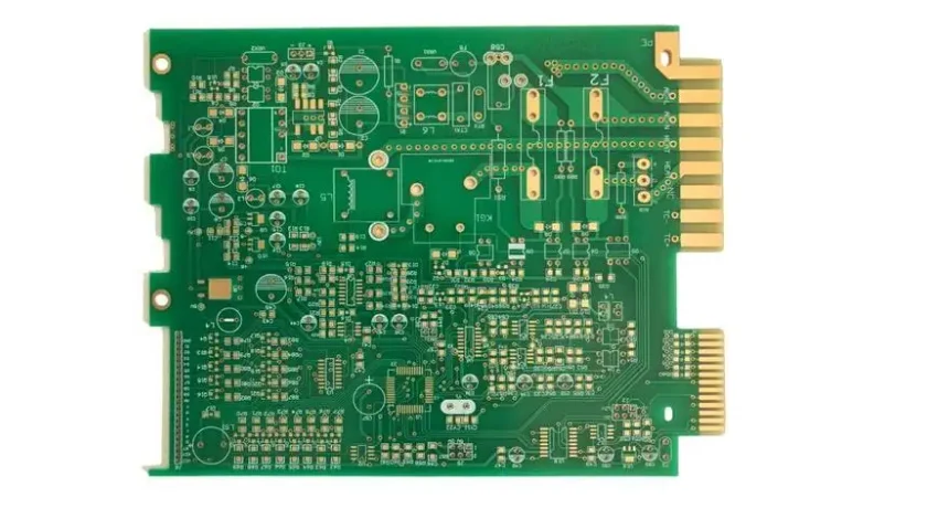
When engineers need reliable circuit boards without the complexity of multilayer designs, double layer FR4 PCBs deliver the perfect balance of functionality and affordability. From consumer electronics to industrial controls, 2-layer boards power millions of devices worldwide while keeping production costs manageable and lead times short.
At HILPCB, we manufacture high-quality FR4 PCBs with precision routing, excellent surface finish, and fast turnaround. Our streamlined production process ensures that your single and double layer PCB projects meet specifications while staying within budget.
Why Double Layer FR4 PCB Dominates the Electronics Industry
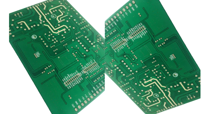
Double layer PCBs feature copper traces on both the top and bottom surfaces, connected through plated-through holes (vias). This simple yet effective design offers significant advantages over single-layer boards while avoiding the expense of multilayer construction.
Key advantages include:
- Increased Routing Density: Both sides available for components and traces, enabling more complex circuits in compact form factors.
- Better Signal Quality: Dedicated ground plane on one layer reduces noise and improves signal integrity.
- Cost Efficiency: Substantially cheaper than 4-layer or 6-layer designs while offering double the routing space.
- Faster Production: Shorter manufacturing cycles mean quicker time-to-market for your products.
- Design Flexibility: Ideal for mixed-signal designs, power distribution, and moderate-density applications.
FR4 material remains the industry standard due to its excellent electrical insulation, mechanical strength, and thermal stability up to 130°C. When combined with double-sided copper, it creates boards that perform reliably across a wide temperature range.
Design Best Practices for Double Layer FR4 PCB
Proper design techniques maximize the performance potential of 2-layer boards while avoiding common pitfalls.
Ground Plane Strategy
Use one entire layer as a ground plane whenever possible. This provides:
- Consistent reference for signal return paths
- Reduced electromagnetic interference (EMI)
- Better power distribution across the board
- Simplified routing for the signal layer
Via Placement and Management
Strategic via placement connects top and bottom layers efficiently:
- Thermal Vias: Dissipate heat from power components to copper pours
- Signal Vias: Route around obstacles and connect components between layers
- Via Stitching: Connect ground pours on both sides for reduced impedance
Use our Gerber Viewer to verify via placement and ensure manufacturing compatibility before production.
Trace Width and Spacing
Calculate appropriate trace widths based on current requirements:
- Signal traces: Typically 0.15mm to 0.3mm for low-current signals
- Power traces: 0.5mm to 2mm depending on current load
- Minimum spacing: 0.15mm for standard production
The Impedance Calculator helps determine exact trace geometry for controlled impedance applications.
Component Placement Strategy
Organize components logically to minimize routing complexity:
- Group related circuits together
- Keep high-frequency components close to reduce trace length
- Position power components with adequate thermal clearance
- Orient connectors for easy access
Manufacturing Excellence for Double Layer FR4 PCB
HILPCB's production capabilities ensure your 2-layer boards meet exact specifications through controlled processes and quality verification.
Advanced Manufacturing Capabilities
Precision Drilling Our CNC drilling equipment maintains ±0.05mm positional accuracy for perfect via alignment and consistent hole quality across the panel.
High-Resolution Imaging LDI (Laser Direct Imaging) systems create precise copper patterns down to 0.1mm trace width with sharp edge definition for improved reliability.
Surface Finish Options Multiple finish choices suit different applications:
- HASL: Cost-effective, excellent solderability
- ENIG: Flat surface, ideal for fine-pitch components
- OSP: Economic choice for immediate assembly
- Immersion Silver/Tin: Balance of cost and performance
Quality Testing Every panel undergoes electrical testing, visual inspection, and dimensional verification before shipping.
Assembly Integration
HILPCB offers complete turnkey solutions from bare boards to assembled products:
- SMT Assembly: Automated placement for surface mount components with 0201 capability
- Through-Hole Assembly: Wave soldering and selective soldering for connectors and legacy parts
- Turnkey Assembly: Complete component sourcing, PCB fabrication, assembly, and testing
- Small Batch Assembly: Flexible production from prototypes to mid-volume runs
Cost Optimization Strategies for Double Layer PCB Projects
Smart design choices significantly impact manufacturing costs without compromising quality.
Panel Utilization
Optimize board dimensions to fit more units per production panel:
- Standard panel sizes: 457mm × 610mm or 400mm × 500mm
- Add V-scoring or routing for easy separation
- Consider panel borders and tooling holes
Material Selection
FR4-TG130 offers the best cost-performance ratio for most applications. Special materials add cost but provide benefits when needed:
- High-Tg FR4: Better thermal stability for lead-free soldering
- Halogen-Free: Environmental compliance for consumer products
- Low-Loss Materials: Improved signal integrity for RF applications
Design for Manufacturing (DFM)
Following manufacturing guidelines reduces cost and improves yield:
- Avoid unnecessarily tight tolerances
- Use standard hole sizes when possible
- Maintain adequate copper-to-edge clearance
- Specify standard material thicknesses
HILPCB – Your Trusted Double Layer FR4 PCB Partner
At HILPCB, we understand that successful products start with reliable circuit boards. Our double layer FR4 PCB manufacturing combines advanced equipment, experienced engineering, and rigorous quality control to deliver boards that meet your exact requirements.
From initial design consultation through final assembly, our team provides comprehensive support at every stage. We offer DFM analysis to optimize your layout, material recommendations for your specific application, and flexible production volumes from prototypes to large-scale manufacturing. Our modern facility houses complete in-house capabilities including drilling, imaging, plating, testing, and assembly—ensuring consistent quality and fast turnaround.
Whether you're developing consumer products, industrial equipment, or automotive systems, HILPCB delivers double layer PCBs with the precision and reliability your project demands. Our commitment to quality, competitive pricing, and customer service has made us the preferred partner for electronics companies worldwide.
Frequently Asked Questions
Q1: What is the difference between single layer and double layer PCB? A single layer PCB has copper traces on only one side, while double layer boards have conductive copper on both top and bottom surfaces connected through plated vias. Double layer designs offer significantly more routing space and better electrical performance.
Q2: How much does a double layer FR4 PCB cost? Pricing depends on board size, quantity, material specification, and surface finish. Typically, 2-layer PCBs cost 30-50% less than 4-layer boards while offering nearly double the routing capacity of single-layer designs. Request a quote for accurate pricing.
Q3: What is the minimum trace width for double layer PCB? Standard manufacturing supports 0.15mm (6 mil) trace width and spacing. For designs requiring tighter tolerances, 0.1mm (4 mil) is achievable with advanced production processes at slightly higher cost.
Q4: Can I use double layer PCB for high-speed signals? Double layer boards work well for moderate-speed digital signals up to 100 MHz. For higher frequencies or strict impedance control requirements, consider 4-layer or 6-layer stackups with dedicated ground planes.
Q5: What copper weight should I specify for my double layer PCB? Standard designs use 1 oz (35 μm) copper. Power applications requiring high current capacity benefit from 2 oz or 3 oz copper weights. Consult with your manufacturer to determine optimal copper thickness for your specific requirements.