
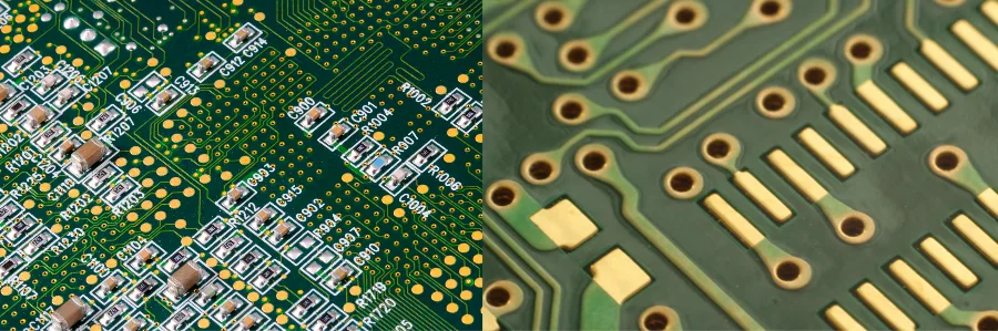
Highleap PCB Factory (HILPCB) delivers exceptional ENIG PCB manufacturing with precise control over electroless nickel and immersion gold deposition. Our advanced chemical processes ensure uniform coating thickness, superior flatness, and excellent solderability for high-reliability applications ranging from fine-pitch BGAs to wire bonding interfaces.
ENIG Process Chemistry and Deposition Mechanisms
The ENIG PCB surface finish involves two distinct chemical processes creating a robust metallic coating system. Understanding these mechanisms enables optimization for specific applications and troubleshooting of potential defects.
Electroless Nickel Deposition
The autocatalytic nickel deposition relies on sodium hypophosphite reducing nickel ions at the copper surface. The reaction proceeds: Ni²⁺ + 2H₂PO₂⁻ + 2H₂O → Ni + 2H₂PO₃⁻ + 2H⁺ + H₂. This creates a nickel-phosphorus alloy typically containing 7-11% phosphorus, determining deposit properties. Medium phosphorus (7-9%) offers optimal balance of hardness, corrosion resistance, and solderability.
Bath parameters critically affect deposition quality. Operating at pH 4.6-4.8 and 85-88°C yields deposition rates of 15-20 μm/hour. Stabilizers prevent spontaneous decomposition while maintaining 4-6 metal turnovers. Our automated dosing systems maintain nickel concentration at 5.5-6.0 g/L and hypophosphite at 25-30 g/L, ensuring consistent coating properties across production runs.
Immersion Gold Reaction
Gold deposition occurs through galvanic displacement: 2Au⁺ + Ni → 2Au + Ni²⁺. This self-limiting reaction typically produces 0.05-0.15 μm gold thickness. The process operates at pH 4.0-4.5 and 80-85°C, with controlled gold concentration of 0.4-0.6 g/L. Complexing agents prevent excessive nickel corrosion while promoting uniform gold distribution.
The immersion reaction's self-limiting nature ensures consistent thickness but requires precise nickel surface preparation. Any passivation or contamination disrupts gold nucleation, creating skip plating defects. Our process includes mild acid activation immediately before gold immersion, guaranteeing complete coverage even on complex HDI PCB designs with fine features.
Design Guidelines for Optimal ENIG Performance
Successful ENIG implementation requires design considerations addressing the finish's unique characteristics and limitations.
Pad Design and Spacing
ENIG's exceptional flatness enables ultra-fine pitch components down to 0.3mm. However, pad design must account for potential nickel corrosion during gold deposition. Maintain minimum pad sizes of 0.25mm diameter for vias and 0.20mm for microvias. Solder mask defined (SMD) pads should include 0.05mm minimum mask overlap preventing edge corrosion.
BGA pad designs benefit from NSMD (non-solder mask defined) configuration with 0.075mm mask clearance. This prevents stress concentration at mask edges while providing optimal solder joint formation. For wire bonding applications, increase pad sizes 20% beyond wire diameter requirements, accounting for potential edge effects during bonding.
Via Treatment Strategies
Via-in-pad designs require careful consideration with ENIG finishes. Filled vias prevent chemistry entrapment but must achieve <25μm dimple depth for reliable solder joints. Through-vias in BGA fields need tenting or filling to prevent solder wicking. Our recommended approach uses conductive via fill for high-speed PCB applications, maintaining signal integrity while ensuring reliable ENIG coverage.
Copper Feature Protection
Large copper areas experience higher corrosion risk during immersion gold deposition. Implement copper thieving patterns with 0.2mm traces spaced 0.5mm apart in sparse regions. This distributes current density during electroless nickel plating, ensuring uniform thickness. Power planes should include multiple connections to prevent isolated areas that may experience skip plating.
Manufacturing Excellence and Process Control
HILPCB's ENIG process control ensures consistent quality meeting IPC-4552 and IPC-6012 specifications through comprehensive monitoring and advanced equipment.
Pre-Treatment Optimization
Surface preparation determines ENIG quality. Our process begins with microetch removing 1-2μm copper, creating uniform texture for nickel adhesion. Sulfuric acid-based cleaners remove organics without attacking the substrate. Critical parameters include:
- Microetch rate: 1.2-1.5 μm/minute
- Surface roughness: Ra 0.3-0.5 μm
- Cleaner temperature: 50-60°C
- Rinse water resistivity: >10 MΩ·cm
Thickness Control Systems
X-ray fluorescence (XRF) measurements at multiple points ensure:
- Nickel thickness: 3-6 μm (typical 5 μm)
- Gold thickness: 0.05-0.15 μm (typical 0.08 μm)
- Phosphorus content: 7-11% by weight
- Thickness uniformity: ±10% across panel
Automated measurement systems check every 10th panel during production, with real-time adjustments maintaining process capability Cpk >1.67. Statistical process control tracks trends, preventing drift before specifications are exceeded.
Quality Verification Methods
Beyond thickness measurements, comprehensive testing validates ENIG integrity:
- Adhesion testing per IPC-TM-650 2.4.1
- Porosity evaluation using nitric acid vapor
- Solderability testing after steam aging
- Cross-sectional analysis for interface examination
- Surface roughness verification for wire bonding
Reliability Considerations and Failure Mechanisms
Understanding ENIG failure modes enables design and process optimization for maximum reliability.
Black Pad Phenomenon
Hyperactivity in immersion gold baths causes excessive nickel corrosion, creating a fractured interface appearing black. Contributing factors include:
- Gold bath pH below 4.0
- Excessive immersion time or temperature
- Contaminated chemistry
- Poor nickel deposit quality
Prevention requires tight process control and regular bath analysis. Our proprietary bath formulation includes grain refiners minimizing corrosion while maintaining deposition rates. Scanning electron microscopy (SEM) inspection of production samples ensures interface integrity.
Brittle Fracture Mechanisms
High phosphorus content (>10%) in electroless nickel creates brittle deposits prone to cracking under thermal stress. This particularly affects heavy copper PCB designs with CTE mismatches. Optimizing phosphorus content at 8-9% balances hardness with ductility, surviving 1000+ thermal cycles without degradation.
Corrosion Resistance Factors
ENIG provides excellent environmental protection when properly applied. However, porous gold deposits allow moisture penetration, initiating nickel corrosion. Minimum gold thickness of 0.05μm ensures adequate coverage, while excessive thickness (>0.20μm) wastes material without improving protection. Mixed flowing gas testing validates corrosion resistance for harsh environment applications.
Why Choose ENIG for Your PCB Surface Finish?
ENIG (Electroless Nickel Immersion Gold) is the ideal surface finish for PCBs requiring superior flatness, reliable solderability, and extended shelf life. Its exceptional performance makes it a top choice for industries like high-frequency electronics, fine-pitch assemblies, and wire bonding applications. ENIG’s uniform coating thickness and excellent corrosion resistance provide consistent and reliable electrical performance for both prototypes and large-volume productions.
Enhanced Performance for High-Speed and High-Density Applications
ENIG’s smooth, gold-plated finish minimizes signal loss and impedance variation, making it perfect for high-frequency circuits. With superior surface flatness, ENIG ensures precise soldering for fine-pitch components like BGAs and QFNs, guaranteeing long-lasting performance even under extreme operating conditions. This finish is particularly advantageous for RF designs, where signal integrity and low loss are critical for optimal functioning.
Durability and Long-Term Reliability
One of ENIG's key benefits is its extended shelf life, maintaining solderability for over 12 months under standard storage conditions. Its resistance to oxidation ensures a long-lasting and robust surface for small-batch assembly, while easy reworkability allows for handling delicate components. Automated assembly processes using ENIG enhance production yields and reduce the risk of defects, making it an excellent solution for manufacturers looking for both reliability and cost-efficiency.
FAQ
What thickness specifications should I request for ENIG PCB? Standard ENIG specifications include 3-6μm nickel and 0.05-0.15μm gold. Most applications perform well with 5μm nickel and 0.08μm gold. Wire bonding requires minimum 0.10μm gold, while cost-sensitive designs may use 0.05μm. Avoid exceeding 0.20μm gold as it provides no additional benefit.
How does ENIG compare to other surface finishes for cost? ENIG costs approximately 15-25% more than HASL but 30-40% less than ENEPIG. For multilayer PCB designs with fine-pitch components, improved yields often offset the higher material cost. The extended shelf life reduces inventory risks compared to OSP finishes.
Can ENIG be reworked or repaired? Limited rework is possible on ENIG surfaces. Localized gold stripping followed by selective replating works for isolated defects. However, large area rework isn't practical due to chemistry selectivity challenges. Design critical features with adequate margin to minimize rework requirements.
What causes solderability issues with ENIG? Poor solderability typically results from nickel passivation due to extended storage in humid conditions or phosphorus enrichment at the surface. Proper packaging with desiccants prevents moisture exposure. Pre-assembly baking at 125°C for 4 hours reactivates marginal surfaces.
Is ENIG suitable for press-fit connectors? ENIG works well for press-fit applications when properly specified. The hard nickel surface (500-600 HV) withstands insertion forces. Ensure minimum 4μm nickel thickness for reliable performance. The smooth surface reduces insertion force compared to HASL finishes.
How do I verify ENIG quality in incoming inspection? Visual inspection should show uniform golden color without cloudiness or discoloration. XRF measurement confirms thickness at multiple locations. Tape testing per IPC-TM-650 2.4.1 verifies adhesion. For critical applications, request cross-sections showing continuous, pore-free coating. Our PCB viewer helps inspect boards remotely before shipping.