Designing reliable flexible circuit boards requires understanding mechanical, electrical, and thermal considerations absent in rigid PCB design. Common mistakes—incorrect bend radius, poor trace routing, or inadequate stress relief—cause premature failures costing time and money. Following proven design practices ensures first-time success.
HILPCB's engineering team provides design support for flexible PCB projects, reviewing layouts, recommending optimizations, and validating designs before manufacturing. Our experience prevents costly mistakes and accelerates time-to-market.
Mechanical Design Fundamentals
Understanding mechanical stress in flexible circuit boards prevents the most common failure modes. Proper design accommodates bending forces while maintaining electrical reliability.
Bend Radius Optimization Calculating minimum bend radius starts with measuring total stack-up thickness including substrate, copper, adhesive, and coverlay. Dynamic-flex applications—where circuits bend repeatedly during operation—require minimum radius of 10× total thickness. Static-flex designs, bent once during assembly, can reduce to 6× thickness. Exceeding these minimums extends flex life dramatically.
Bend axis placement critically impacts reliability. Position bends away from vias, which create stress concentration points. When vias in bend regions are unavoidable, tear-drop via pads distribute stress more evenly than standard circular pads. Consider via-free zones in high-stress areas.
Stiffener Design Strategy Areas requiring component mounting, connectors, or ZIF interfaces need reinforcement. Polyimide or FR4 stiffeners laminate to flex circuits providing rigid platforms. Proper stiffener design includes:
- Rounded corners (minimum 3mm radius) preventing stress concentration
- Gradual thickness transitions from flex to rigid regions
- Adhesive selection matching operating temperature requirements
- Cutouts for components exceeding stiffener height
Trace Routing and Layer Stack-Up
Electrical design for flexible circuits differs significantly from rigid PCB layout. Trace geometry, layer arrangement, and via placement directly affect mechanical reliability.
Trace Routing Best Practices Route traces perpendicular to bend axis when possible. Traces parallel to bending experience maximum stress, causing copper fatigue and cracking. In curved sections, use I-beam pattern (straight segments with radiused corners) rather than constant curves to distribute stress evenly.
Avoid trace necking in flex regions. Narrower traces concentrate stress and fail faster. Maintain consistent widths or gradually taper when width changes are necessary. Space traces adequately—closer spacing reduces flexibility due to increased copper density.
Hatched ground planes instead of solid copper in flex regions maintain flexibility while providing shielding. 50-70% copper coverage balances electrical performance with mechanical flexibility. Solid planes appropriate only in rigid sections.
Multilayer Stack-Up Design Multi-layer flexible boards require careful layer arrangement. Position copper layers symmetrically around substrate centerline to balance stresses during bending. Asymmetric constructions cause preferential bending direction and premature failure.
For four-layer flex: Signal-Ground-Power-Signal arrangement provides good impedance control and EMI shielding. Six-layer construction adds routing density while maintaining flexibility through thin copper weights (½ oz or ¼ oz). Polyimide material selection impacts dielectric constant and loss tangent for high-speed signals.
Component Integration and Assembly
Placing components on flexible circuit boards requires considerations beyond standard rigid PCB assembly. Mechanical stress, thermal management, and accessibility affect component reliability.
Component Placement Strategy Never place components directly in bend regions. Bending stress transfers to solder joints causing cracking and electrical failure. Use stiffeners under all components providing stable mounting platforms. Stiffener thickness should equal or exceed component height preventing excessive flexing under handling forces.
SMT component orientation matters on flex circuits. Position components with long axis perpendicular to bend direction when possible. This minimizes stress on solder joints during flexing. Use smaller package sizes (0402, 0201) which better tolerate flex compared to larger components.
Thermal Management Considerations Flexible PCB materials conduct heat poorly compared to thick copper rigid boards. Power components require thermal vias transferring heat through stack-up to external surfaces. Consider thermal pads or metal stiffeners under high-power components acting as heat spreaders.
Operating temperature affects material selection. Standard polyimide operates to +150°C continuously, suitable for most applications. Higher temperatures require high-performance polyimide grades or ceramic-filled substrates.
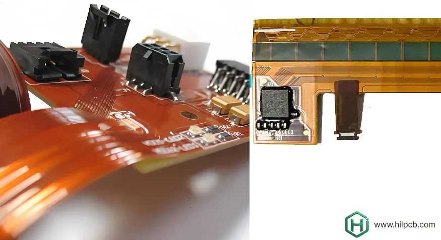
Connector and Interface Design Connector footprints require precise dimensional accuracy. ZIF (Zero Insertion Force) connectors demand tight tolerance on gold finger dimensions and spacing. Manufacturing capabilities typically maintain ±0.1mm tolerance; specify accordingly.
Gold finger plating thickness affects insertion cycles. Specify 0.05-0.10μm gold over 1-3μm nickel for standard applications. Increase gold thickness to 0.10-0.15μm for high-cycle applications (>1000 insertions). Hard gold plating provides better wear resistance than soft gold.
HILPCB — Flexible Circuit Board Design and Engineering Excellence
HILPCB provides complete design and manufacturing support for Flexible Circuit Boards, helping engineers turn complex concepts into reliable, production-ready solutions. Our Gerber Viewer tool enables real-time file verification, ensuring every flexible PCB design meets mechanical, electrical, and fabrication standards before production begins. Detailed engineering reviews evaluate bend radius, via positioning, and material balance to guarantee long-term durability and manufacturability.
With experience across consumer electronics, medical, automotive, and aerospace industries, HILPCB combines Flexible Circuit Board expertise with advanced FPC design knowledge to deliver high-performance interconnect solutions. Each project benefits from precise material selection, controlled impedance stack-ups, and quick-turn prototyping that accelerates validation while minimizing cost. Our integrated workflow bridges the gap between design and production, ensuring consistent quality at every stage.
Partnering with HILPCB means working with a trusted Flexible Circuit Board manufacturer dedicated to engineering excellence. We act as an extension of your design team—streamlining development, reducing risk, and accelerating time-to-market. Let our experts optimize your next flex PCB design and bring innovation to life with confidence.
Frequently Asked Questions
Q1: What is the minimum bend radius I should design for? Dynamic-flex applications require 10× total thickness minimum radius. Static-flex (bent once during assembly) can use 6× thickness. Measure total thickness including substrate, copper, adhesive, and coverlay. Larger radius improves reliability—use 15-20× thickness when space permits.
Q2: Can I place components in flexible circuit board bend regions? No, never place components directly in bend areas. Bending stress causes solder joint cracking and component failure. Use stiffeners under all components providing rigid mounting platforms. Separate flex interconnect sections from rigid component mounting areas.
Q3: How do I design gold fingers for connector interfaces? Specify gold finger dimensions per connector manufacturer requirements. Typical specifications: 0.05-0.10μm gold plating over 1-3μm nickel, ±0.05mm dimensional tolerance, 1.5mm minimum finger length. Beveled edges (30-45°) ease connector insertion. Hard gold plating recommended for high insertion cycles.
Q4: Should I use solid or hatched copper fills in flex regions? Use hatched copper fills (50-70% coverage) in bend regions maintaining flexibility while providing ground planes. Solid copper planes appropriate only in rigid sections with stiffeners. Cross-hatched pattern at 45° angle distributes stress evenly.
Q5: What trace width should I use in flexible circuit boards? Specify wider traces than equivalent rigid PCB design. Minimum 150μm (6 mil) width in flex regions recommended for reliability. Wider traces (200-300μm) improve flex life significantly. Avoid trace width changes in bend regions—maintain consistent width through bending areas.