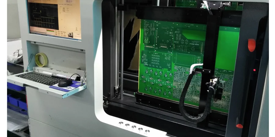
Highleap PCB Factory (HILPCB) delivers cutting-edge flying probe testing capabilities that provide unparalleled flexibility in PCB quality assurance. Our advanced testing infrastructure combines precision probe positioning, intelligent test sequencing, and comprehensive fault detection to ensure optimal product reliability across diverse electronic applications without the constraints of traditional fixture-based testing approaches.
Flying Probe Testing Core Principles and Technology Architecture
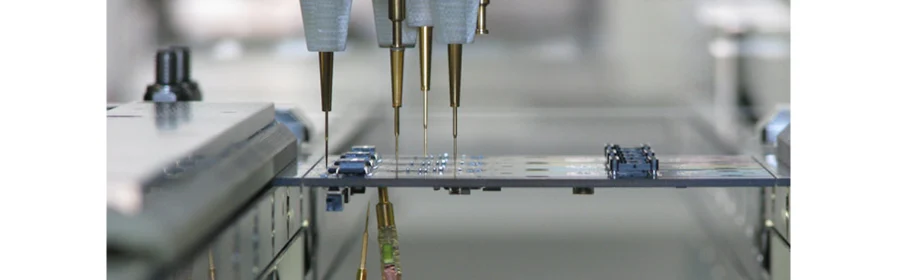
Flying probe testing represents a sophisticated non-fixture approach to PCB quality verification that employs multiple movable test probes capable of accessing virtually any exposed conductor on assembled boards. This technology eliminates the traditional dependency on custom test fixtures while maintaining comprehensive electrical testing capabilities through precision mechanical positioning and advanced measurement algorithms.
Advanced Flying Probe Testing Technologies:
• Precision Mechanical Positioning: Servo-controlled probe assemblies achieve positioning accuracies within micrometers, enabling reliable contact with fine-pitch components and dense interconnection patterns through linear motor drives or precision ball screw assemblies • Specialized Probe Technology: Spring-loaded probe tips with tungsten carbide or diamond-coated surfaces provide controlled contact force while maintaining electrical integrity across thousands of test cycles without component damage • Multi-Instrument Integration: Electrical measurement subsystems combine precision digital multimeters, signal generators, and specialized test circuits with high-speed switching matrices for rapid measurement reconfiguration • Boundary Scan Capabilities: IEEE 1149.1 compliant testing enables comprehensive verification of complex digital components without requiring direct probe access to individual component pins • Intelligent Test Sequencing: Path optimization algorithms consider mechanical constraints, electrical isolation requirements, and measurement dependencies to generate efficient test sequences that minimize execution time • Guard-Driving Techniques: Advanced measurement isolation prevents interference from adjacent circuit nodes during precision electrical parameter verification • Real-Time Feedback Control: Dynamic adjustment of probe positioning and contact force based on surface topology variations and component height differences • Machine Learning Optimization: Historical test data analysis continuously improves sequencing efficiency and identifies optimal measurement parameters for specific board configurations • Environmental Adaptation: Adaptive capability proves particularly valuable when testing flex PCB assemblies where dimensional variations require continuous position compensation
Strategic Flying Probe Implementation: Modern flying probe testing platforms integrate multiple advanced technologies enabling comprehensive fault detection while optimizing test execution efficiency. Our China PCB manufacturing expertise ensures optimal flying probe testing integration tailored to your specific quality requirements and production flexibility demands.
Flying Probe Testing vs Traditional ICT Methods
The comparison between flying probe testing and conventional bed-of-nails ICT approaches reveals distinct advantages and limitations that influence methodology selection based on specific manufacturing requirements and product characteristics.
Flexibility and Setup Considerations:
Flying probe testing eliminates the requirement for custom test fixtures, providing immediate testing capability for new product designs without the lead time and cost associated with fixture development. This flexibility proves particularly advantageous for small-batch assembly operations where fixture costs cannot be amortized across large production volumes. The absence of fixture requirements also enables testing of boards with non-standard configurations, unusual form factors, or components that would interfere with traditional fixture assemblies.
Test Coverage and Accessibility:
While bed-of-nails systems provide simultaneous access to multiple test points, flying probe systems can reach virtually any exposed conductor regardless of board layout constraints. This capability enables comprehensive testing of HDI PCB designs where high component density and fine-pitch interconnections limit traditional test point placement. Flying probe systems excel in accessing test points located beneath components, along board edges, or in areas where fixture probe placement would be mechanically impossible.
Throughput and Production Volume Considerations:
Traditional ICT systems typically achieve higher throughput for standardized production due to simultaneous multi-point testing capabilities. Flying probe systems compensate for sequential testing limitations through intelligent test optimization and parallel probe operation where multiple probes can perform independent measurements simultaneously. Modern flying probe systems achieve throughput rates approaching traditional ICT for many applications while maintaining superior flexibility for design variations.
Measurement Accuracy and Reliability:
Both methodologies achieve comparable measurement accuracy for standard electrical parameters. Flying probe systems may demonstrate superior performance in applications requiring precise probe positioning or when testing components sensitive to mechanical stress from fixture loading. The dynamic contact force control available in flying probe systems enables optimization of contact conditions for different surface finishes and component types.
Economic Analysis and Cost Effectiveness:
The economic comparison between flying probe and traditional ICT depends heavily on production volume and product mix variability. Flying probe systems demonstrate clear advantages for low-volume production, prototype testing, and applications with frequent design changes. Traditional ICT becomes more cost-effective as production volumes increase and product designs stabilize, allowing fixture costs to be distributed across larger quantities.
How to Optimize Flying Probe Testing for Reliable and Efficient PCB Quality Control
Flying probe testing is not just about detecting faults—it's about doing it quickly, accurately, and consistently. At Highleap PCB Factory, we focus on optimizing every aspect of this process to enhance reliability and reduce test time, especially for complex or low-volume PCB assemblies.
Intelligent Test Program Generation
We start by analyzing your PCB’s CAD and netlist data to automatically generate a highly efficient test plan. Our software identifies all accessible test points, simulates the sequence, and checks for issues like missing nets or inaccessible nodes. This automation reduces human error and speeds up deployment—ideal for prototyping and fast-moving production cycles.
Process Monitoring and Quality Tracking
Our flying probe systems are equipped with real-time monitoring and statistical process control (SPC). This means we’re not just running tests—we’re watching for trends. If a specific failure mode starts recurring, the system flags it immediately. We track:
- Test coverage and execution time
- Pass/fail rates per board
- Repeatability of critical measurements
This feedback loop helps ensure every board meets the same high quality standard.
Maintenance for Long-Term Accuracy
Precision testing depends on precise tools. We maintain our flying probe machines with strict daily and monthly schedules:
- Daily tip cleaning and alignment checks
- Monthly mechanical calibration of the X-Y-Z axes
- Scheduled probe tip replacement based on contact cycles
These practices ensure stable contact quality and measurement accuracy throughout high-volume test operations.
Smart Integration with Manufacturing Systems
To support traceability and fast feedback loops, we integrate our testers with your manufacturing execution systems (MES). This allows automatic test result logging, immediate notification of failures, and even design-based test updates when you change your Gerber files. You can also preview the board in our Gerber Viewer to verify any test coverage assumptions.
Why Choose Highleap PCB Factory for Professional Flying Probe Testing
Advanced Testing Infrastructure for Diverse PCB Requirements Highleap PCB Factory (HILPCB) offers industry-leading flying probe testing backed by precision equipment and adaptable systems. Our facility operates next-generation flying probe testers capable of sub-micrometer accuracy, supporting high-density layouts and varied board geometries. These systems enable reliable testing without the need for custom fixtures, making them ideal for prototype verification, low- to mid-volume production, and fine-pitch assemblies. Automated test generation, CAD-based analysis, and environmental control chambers further enhance the effectiveness of our testing process across product lifecycles.
Specialized Engineering Expertise and Design Collaboration Our in-house engineering team provides comprehensive test program development and consulting services tailored to complex board assemblies. This includes design for testability (DFT) reviews, netlist-based fault isolation planning, and parametric test optimization. Whether working with HDI PCB or multilayer PCB designs, we collaborate closely with clients to ensure maximum fault coverage with minimal development time. Our engineers also support rapid adaptation to design changes and frequent iteration common in agile product development.
Integrated Quality Systems and Scalable Production Support Flying probe testing at HILPCB is fully embedded within our ISO 9001-certified quality management system. Test data is automatically recorded and analyzed using real-time statistical process control (SPC), enabling traceability and early defect detection. Combined with automated reporting tools, this infrastructure ensures compliance with industry standards and customer-specific quality protocols. Additionally, our systems are optimized for flexibility, supporting everything from engineering validation builds to large-volume production runs with frequent changeovers and diverse testing criteria.
FAQ
What are the main advantages of flying probe testing over traditional ICT methods? Flying probe testing offers superior flexibility by eliminating custom fixture requirements, enabling immediate testing of new designs without lead time delays. The technology provides access to virtually any exposed conductor regardless of board layout constraints, making it ideal for complex layouts, unusual form factors, and high-density assemblies where traditional fixture placement would be impossible.
How does flying probe testing handle fine-pitch components and dense assemblies? Modern flying probe systems achieve positioning accuracies within micrometers, enabling reliable contact with components down to 0.2mm pitch and smaller. Specialized probe tip designs and controlled contact force mechanisms ensure reliable electrical connection while minimizing risk of component damage. Advanced systems incorporate vision systems for precise probe positioning on small targets.
What factors determine flying probe testing speed and throughput? Test execution speed depends on board complexity, number of test points, probe movement optimization, and measurement requirements. Modern systems employ intelligent path optimization algorithms that minimize probe travel time while multiple probe configurations enable parallel testing operations. Typical test times range from 30 seconds for simple boards to several minutes for complex assemblies.
Can flying probe testing verify complex digital circuits and processors? Yes, advanced flying probe systems integrate boundary scan testing capabilities that enable comprehensive verification of digital components without requiring direct probe access to individual pins. This capability combined with traditional electrical measurements provides complete testing coverage for complex mixed-signal assemblies including microprocessors, FPGAs, and other advanced digital components.
How does flying probe testing compare economically to traditional ICT for different production volumes? Flying probe testing demonstrates clear economic advantages for low-volume production, prototypes, and applications with frequent design changes due to elimination of fixture costs. Break-even analysis typically favors flying probe for quantities below 1000-5000 units annually, though exact volumes depend on board complexity and testing requirements. Traditional ICT becomes more cost-effective for high-volume standardized production.
What maintenance requirements are necessary for flying probe testing systems? Flying probe systems require regular calibration of positioning mechanisms, probe tip replacement based on contact cycles, and periodic verification using reference standards. Daily cleaning protocols maintain probe tip condition while monthly mechanical calibration ensures positioning accuracy. Preventive maintenance schedules typically include quarterly comprehensive system verification and annual factory calibration procedures.