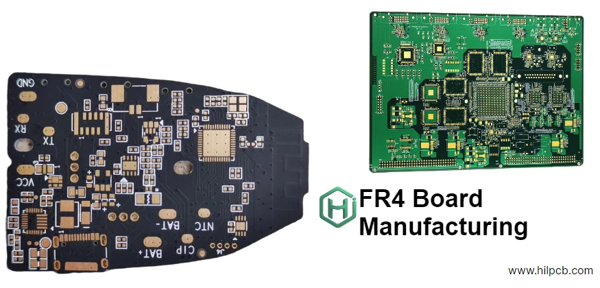
Selecting the right FR4 board — also known internationally as an FR4 PCB, FR4 circuit board, or FR4 printed circuit board — directly determines how your product performs, how easy it is to assemble, and how much it costs. Some engineers even refer to it as an FR4 substrate or glass-epoxy PCB, since it’s made of woven fiberglass cloth and epoxy resin reinforced with flame-retardant additives.
This guide from HilPCB explains what really matters when choosing an FR4 board: material grade, stack-up design, copper planning, cost control, and DFM preparation — so you can move confidently from prototype to mass production.
1. Why FR4 Boards Remain the Industry Default
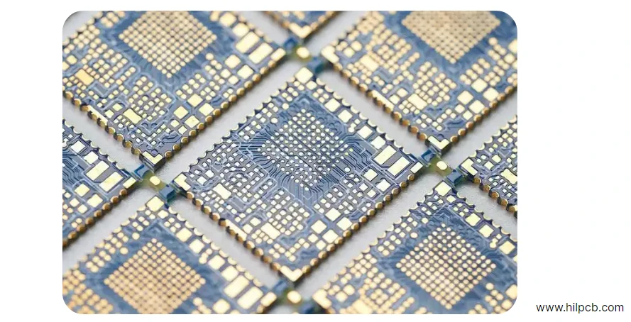
The FR4 board (or FR4 PCB) remains the world’s most widely used printed circuit board material, striking the perfect balance between cost, mechanical strength, and electrical stability. It supports everything from low-cost consumer gadgets to industrial controllers and RF modules, making it the logical starting point for nearly every electronics project.
When your design scales, you usually extend FR4 technology instead of switching to exotic dielectrics:
- Increase layer count → multilayer PCB
- Localize density under fine-pitch BGAs → HDI PCB
- Integrate component placement → SMT assembly
HilPCB delivers end-to-end PCB manufacturing and assembly—covering FR4, high-Tg/low-loss FR4, high-frequency laminates, and complex multilayer/HDI builds—backed by rigorous quality control and full material traceability.
2. FR4 Material Options and When to Use Them
| FR4 Type | Tg Range | Typical Use | Notes |
|---|---|---|---|
| Standard FR4 | 130–140 °C | Consumer, IoT, industrial control | Most cost-efficient |
| Mid-Tg FR4 | 150–160 °C | LED lighting, automotive | Better reflow tolerance |
| High-Tg FR4 | 170–180 °C | Multilayer, fine-pitch BGA | Lower expansion, stable yield |
| Low-Loss FR4 | ~170 °C | High-speed & RF | Df ≤ 0.012 for clean signals |
| Halogen-Free FR4 | 150–170 °C | Green compliance | Required for EU/telecom |
Tip: Always pick the lowest grade that safely meets your temperature, frequency, and reflow needs — over-spec adds cost without reliability gain.
3. Stack-Up, Copper & Impedance Planning — The Core of a Reliable FR4 Board
This is where a good FR4 design becomes a great one. Stack-up definition determines impedance accuracy, heat distribution, EMI behavior, and yield. At HilPCB, 70% of DFM corrections relate to incomplete or unrealistic stack-up data, so this stage deserves attention.
a) Layer & Dielectric Design
- 4 to 6 layers cover most FR4 boards.
- Use 1.6 mm total thickness unless space or mechanical limits apply.
- Maintain symmetry (e.g., core-prepreg-core-prepreg) to avoid warpage.
- Define plane pairs (GND–PWR) close to signal layers to stabilize impedance.
Typical 4-layer FR4 stack-up example:
1 oz Cu + 0.18 mm prepreg + 1 oz Cu (core) + 0.18 mm prepreg + 1 oz Cu
→ total thickness ≈ 1.6 mm, dielectric ≈ 0.32 mm, impedance ≈ 50 Ω single / 100 Ω diff.
b) Copper Weight Strategy
- Outer layers: 1 oz for fine-pitch soldering and routing.
- Inner planes: 2–3 oz for power distribution or heat spreading.
- Heavy copper (>3 oz) requires wider trace/space and controlled etch compensation — specify clearly in fab notes.
Balanced copper helps prevent bow and twist during lamination.
c) Impedance Control on FR4
FR4’s dielectric constant (Dk ≈ 4.2–4.6) varies with resin content and frequency.
To maintain < ±10 % impedance variation:
- Fix trace geometry early with HilPCB’s impedance calculator.
- Choose low-loss FR4 (Df < 0.012) for 2–10 GHz signals.
- Include impedance coupons on every panel for TDR sampling.
d) Thermal & Mechanical Balance
FR4’s thermal conductivity (~0.3 W/m·K) limits heat spread, so use:
- Thick copper planes under power devices,
- Thermal vias near heat sources,
- High-Tg FR4 to reduce Z-axis expansion (50 → 45 ppm/°C).
A balanced stack-up with symmetrical copper reduces reflow stress and improves yield.
4. Cost, Lead Time & Quality Factors
Cost levers:
- Reduce unnecessary layers or HDI zones.
- Align FR4 board outlines to standard panels.
- Use Immersion Silver/Tin instead of ENIG for non-fine-pitch projects.
- Combine multiple small designs into one panel for prototyping.
Typical lead times:
- 2–4 layer FR4 boards: 5–7 working days
- 6–12 layer FR4 boards: 10–12 days
- Volume production: 12–15 days (expedite on request)
Quality checkpoints:
HilPCB runs 100 % electrical test, AOI, and optional X-ray.
All materials meet UL 94 V-0 and IPC-4101 standards.
Learn more in our PCB manufacturing overview.
5. How to Get a Fast, Accurate FR4 Board Quote
No matter if you’re a buyer collecting pricing or an engineer preparing files, we make it simple to get a clear, accurate quote for your FR4 board (also called FR4 PCB or FR4 circuit board). You don’t need to have every file ready — just send what you already have, and our engineers will handle the rest.
What You Can Send
- Gerber / ODB++ / CAD file — any format from Altium, KiCad, Eagle, or others
- BOM (Bill of Materials) — even a partial list helps us prepare the assembly quote
- Board specs if you don’t have design files: layer count, board size, thickness (e.g., 1.6 mm), copper weight, and surface finish
- Special requirements: controlled impedance, high-frequency materials, or HDI features
- Quantity and target delivery time
What Happens Next
Once we receive your information, our engineering team will:
- Review your files for manufacturability (DFM)
- Recommend suitable FR4 materials and stack-up configuration
- Confirm whether assembly is required
- Provide a detailed quotation and lead time within 24 hours
If anything is missing, we’ll guide you step-by-step — no technical experience required.
Whether you’re starting from a concept, CAD layout, or complete data pack, HilPCB ensures every FR4 PCB quotation includes verified materials, a manufacturable design, and a reliable delivery schedule.