Gold finger PCBs are critical in the development of high-quality electronic connectors, ensuring reliable and high-performance connections in a wide range of applications. The gold plating on the PCB edges, known as “gold fingers,” allows for a secure and low-resistance connection to another component or board, making it an essential element in modular electronics, telecommunications, and advanced computing systems.
At Highleap PCB Factory, we specialize in the design and manufacturing of Gold Finger PCBs for a variety of high-performance applications. Our expertise in advanced PCB technologies, including high-density designs and special material systems, ensures that your project will meet its required electrical and mechanical specifications.
What is a Gold Finger PCB?
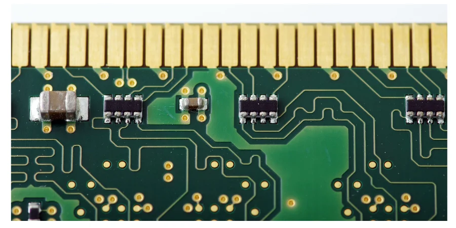
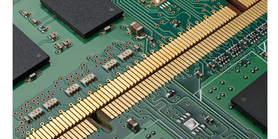
A Gold Finger PCB is a type of printed circuit board that features gold-plated pads along the edge of the board. These gold fingers provide a highly durable and corrosion-resistant interface for connecting the PCB to other components, typically through edge connectors. Gold finger connectors are essential for high-speed data transfer and applications that require a reliable, low-resistance connection.
Gold finger PCBs are widely used in:
- Modular systems: Where the PCB connects to a larger system or backplane, such as in telecom equipment, memory modules, or GPUs.
- High-speed computing systems: Where signal integrity is crucial, such as in networking cards, memory expansion cards, and graphic cards.
- Consumer electronics: In applications such as gaming consoles, computer peripherals, and high-performance storage devices.
Highleap PCB Factory’s Gold Finger PCBs are designed to handle these demanding applications, providing high-quality, reliable connectors with low insertion loss and superior mechanical strength.
Manufacturing Process for Gold Finger PCBs
Manufacturing Gold Finger PCBs involves a series of precise steps to ensure the correct plating, shape, and finish for the gold-plated pads:
- Design: Our engineering team works closely with you to ensure that the gold finger layout fits your specific requirements, including pad size, spacing, and board geometry.
- Plating: We use high-quality gold plating to coat the edge pads, ensuring a durable and corrosion-resistant surface for reliable electrical connections.
- Impedance Control: For high-speed and high-frequency applications, impedance matching is critical. We leverage advanced tools such as the Impedance Calculator to ensure optimal signal integrity in your Gold Finger PCB design.
- Edge preparation: We precisely mill the edges of the PCB to ensure that the gold-plated pads align perfectly with connectors, achieving a tight, reliable fit.
Our in-house Gerber Viewer and 3D PCB Viewer allow for precise design verification, ensuring that the final product meets your design specifications before production.
Applications of Gold Finger PCBs
Gold finger PCBs are used in a variety of industries where reliable and high-speed data transmission is required. Common applications include:
- Telecommunications Equipment: Gold finger PCBs are commonly used in telecom systems to connect communication boards to backplanes, ensuring high-speed data transmission with minimal signal degradation.
- Graphics Cards and Memory Modules: In computing, Gold Finger PCBs are used in memory expansion cards, GPUs, and other peripherals where fast and reliable signal connections are necessary.
- Automotive Electronics: Automotive systems, including ECUs (Electronic Control Units) and diagnostic tools, use Gold Finger PCBs for reliable interconnectivity in rugged environments.
- Networking: High-speed networking equipment such as switches, routers, and network cards rely on Gold Finger PCBs to connect to backplanes or other system components.
At Highleap PCB Factory, we ensure that our Gold Finger PCBs are tailored for the specific mechanical and electrical requirements of each application, whether it’s for high-frequency or power-sensitive systems.
Why Choose Highleap PCB Factory for Your Gold Finger PCB Needs?
Highleap PCB Factory stands out as a trusted Gold Finger PCB manufacturer, offering several key advantages:
- Custom Solutions: We provide tailored solutions for your unique design requirements, ensuring the gold finger pads meet your performance, mechanical, and electrical standards.
- Advanced Materials: We work with a wide range of high-quality materials, including high-Tg PCB, flex PCB, and metal-core PCBs to meet specific electrical and thermal requirements.
- Precision Manufacturing: Our precision manufacturing processes, such as laser cutting and advanced plating, ensure high-quality Gold Finger PCBs with reliable mechanical strength and low signal attenuation.
- Fast Turnaround: We provide quick prototyping and fast turnaround times for both low and high-volume orders, with the ability to scale production to meet your business needs.
- Comprehensive Testing: We conduct thorough testing at every stage of production to ensure that the final product meets your specifications for electrical performance, reliability, and durability.
We are committed to delivering Gold Finger PCBs that perform flawlessly in the most demanding environments.