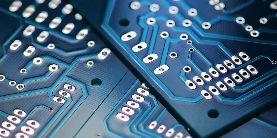
Highleap PCB Factory (HILPCB) has perfected Hot Air Solder Leveling (HASL) processes over two decades of manufacturing excellence. Our expertise in both traditional and lead-free HASL PCB finishes ensures optimal solderability and long-term reliability for diverse applications, from consumer electronics to industrial control systems requiring robust, cost-effective surface treatments.
HASL Process Fundamentals and Technical Parameters
Hot Air Solder Leveling involves immersing bare copper PCBs in molten solder at 250-275°C, then using high-pressure air knives to level the coating. Critical process parameters include:
- Pre-heating: 100-120°C prevents thermal shock
- Solder temperature: 250-265°C (leaded) or 260-275°C (lead-free)
- Air pressure: 20-30 PSI at 45-60° angle
- Withdrawal speed: 25-50 inches/minute
- Coating thickness: 1-25μm per IPC-4552
Temperature differentials must not exceed 150°C to prevent warpage in multilayer PCB designs. Our process engineers optimize parameters based on board characteristics - thickness, hole density, and copper weight - ensuring consistent coverage while minimizing thickness variations.
The solder alloy fundamentally impacts results. Traditional 63/37 tin-lead melts at 183°C, while lead-free SAC305 (Sn96.5/Ag3.0/Cu0.5) requires 217-220°C. Higher lead-free temperatures demand tighter control and may exclude temperature-sensitive substrates.
Comparing Leaded vs Lead-Free HASL Technologies
The transition from leaded to lead-free HASL represents more than regulatory compliance - it fundamentally alters process dynamics and application suitability. Understanding these differences enables informed selection for specific project requirements.
Metallurgical Characteristics
Leaded HASL forms intermetallic compounds (IMCs) of Cu6Sn5 and Cu3Sn at the copper interface, growing predictably at 1-2μm during standard reflow cycles. Lead-free SAC alloys create similar IMCs but with accelerated growth rates, reaching 3-5μm after equivalent thermal exposure. This faster IMC formation can benefit initial soldering but may compromise long-term reliability in high-temperature applications.
Thermal Cycling Performance
Extensive testing reveals distinct failure modes between HASL types. Leaded coatings exhibit gradual degradation through 1000+ thermal cycles (-40°C to +125°C), maintaining acceptable solder joint strength. Lead-free HASL shows superior initial strength but experiences more rapid degradation after 500-750 cycles due to increased brittleness and IMC growth. For heavy copper PCB applications with extreme thermal mass, these differences become particularly pronounced.
Surface Planarity Considerations
HASL inherently creates uneven surfaces due to solder surface tension effects. Leaded HASL typically achieves 10-25μm thickness variation across a board, while lead-free variants show 15-40μm variation due to higher surface tension. This non-planarity limits HASL suitability for fine-pitch components below 0.5mm pitch, where coplanarity requirements demand alternative finishes like ENIG or immersion silver.
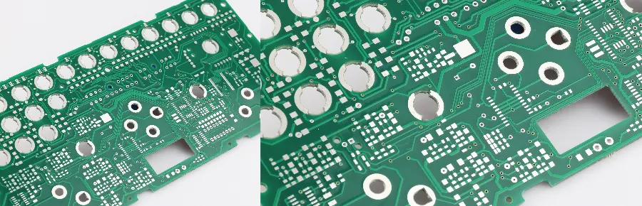
PCB Design Optimization for HASL Surface Finish
Smart design choices dramatically improve HASL results and assembly yields:
Pad Design Guidelines
- Reduce SMD pad sizes 10-20% versus ENIG designs
- BGA pads: Design at 0.38-0.40mm for 0.45mm nominal
- Aspect ratios: Keep rectangular pads between 1:1 and 1:1.5
- Add 0.3mm solder thieves near critical pads for distribution control
Panel Configuration
- Orient longest dimension vertically during processing
- Position fine-pitch components >20mm from panel edges
- Use 3-5mm copper balance borders on large panels
- Tab-routing preferred over V-scoring for thermal isolation
Thermal Management
- Implement 0.2-0.3mm thermal relief spokes on large copper areas
- Maintain 0.4mm clearance between planes and pad edges
- Balance copper distribution to prevent differential heating
- For heavy copper PCB, use selective relief patterns
Quality Control and Manufacturing Excellence
HILPCB's comprehensive quality systems ensure consistent HASL performance:
Process Monitoring
- Solder pot temperature: ±2°C precision
- Contamination: <0.1% copper content
- Automated optical inspection post-HASL
- Statistical control maintaining Cpk >1.33
Reliability Testing
- Solderability per IPC J-STD-003
- Steam aging 8 hours simulating storage
- Wetting balance >75% at 245°C (255°C lead-free)
- Thermal shock -55°C to +125°C for 500 cycles
- Salt spray 96+ hours per ASTM B117
Application Validation
- Consumer electronics: Selective HASL reduces costs 30-40% versus full ENIG
- Industrial systems: Superior durability for harsh environments
- Automotive: Meets AEC-Q100 when properly implemented
- Prototypes: Immediate availability and reworkability advantage
Partner with HILPCB for Superior HASL PCB Solutions
When reliability meets cost-effectiveness, HILPCB delivers exceptional HASL PCB manufacturing. Our state-of-the-art facility combines decades of expertise with modern automation, ensuring every board exceeds IPC Class 2 requirements. Free design reviews help optimize your layouts for HASL processing, improving yields while reducing costs.
We accommodate everything from single prototypes to millions of units annually, maintaining consistent quality across all volumes. Our turnkey assembly services integrate seamlessly with HASL boards, delivering complete solutions optimized for your specific requirements. Engineering support identifies potential challenges before production, helping customers reduce field failures by up to 75%.
FAQ
What component limitations exist for HASL PCB assembly? HASL works reliably with 0.5mm pitch QFPs and 0.8mm pitch BGAs. Finer pitches risk opens due to coplanarity variations. Consider mixed finishes - HASL for general areas with ENIG for fine-pitch zones.
How does HASL compare to other finishes for cost? HASL costs 50-70% less than ENIG while providing superior shelf life versus OSP. For large-volume assembly, the savings are substantial. Initial tooling costs are minimal compared to selective plating options.
Can HASL work with high-frequency designs? HASL's thickness variations create impedance discontinuities above 1 GHz. For high-frequency PCB applications, use ENIG or immersion silver on RF sections while applying HASL to power and digital areas.
What causes excessive HASL thickness on small pads? Surface tension naturally accumulates more solder on confined geometries. Design solutions include enlarging pads where possible, adding thermal reliefs, and incorporating solder thieves. Our process optimization minimizes but cannot eliminate this physical characteristic.
Is lead-free HASL suitable for all PCB materials? Standard FR-4 PCB handles lead-free temperatures well. Low-Tg materials risk delamination. High-frequency laminates vary - verify ratings exceed 280°C. Flex and rigid-flex typically require alternative finishes due to temperature limitations.
How should I specify HASL in design files? Note "HASL" or "Lead-free HASL" in fabrication drawings per IPC-4552. Use our Gerber viewer to verify specifications. Include any selective finish requirements on mechanical layers. Avoid over-specifying thickness - standard processes provide adequate coverage for most applications.