The 5G revolution demands unprecedented circuit density—base station radio units pack 64+ antenna elements, each requiring precise RF routing and controlled impedance interconnections into board areas barely 300mm square. Traditional PCB technology simply cannot achieve this density while maintaining signal integrity at millimeter-wave frequencies.
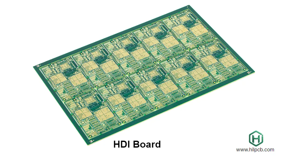
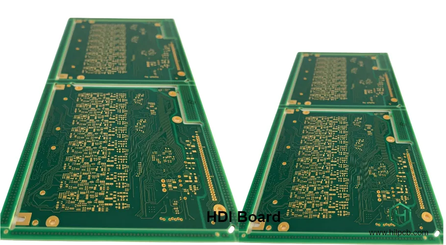
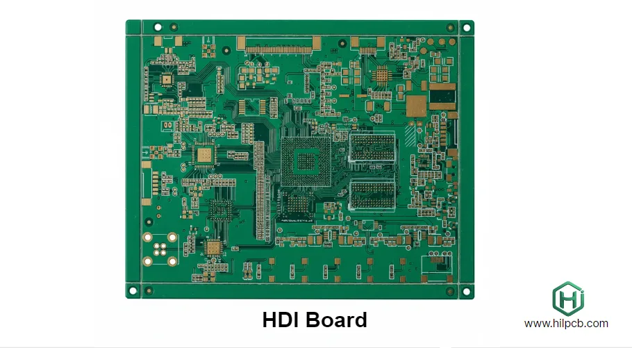
HDI board technology solves this challenge through laser-drilled microvias, ultra-thin dielectrics, and advanced high-frequency materials that enable routing densities 3-5x beyond conventional multilayer approaches. At HILPCB, we manufacture HDI boards for demanding wireless, 5G, radar, and high-speed digital applications alongside our complete range of Rogers laminates and PTFE substrates. Our integrated services cover design optimization, precision fabrication, and complete assembly for complex RF systems.
RF Performance Optimization in HDI Board Designs
Controlled Impedance in High-Density Routing
Maintaining precise 50-ohm or differential impedance becomes significantly more challenging in HDI boards where thin dielectrics and fine traces create larger manufacturing tolerances as percentage of target values.
Impedance Control Strategies:
Conventional boards use 0.100mm or thicker dielectrics between signal layers and reference planes—providing generous tolerance windows. HDI build-up layers may be only 0.050mm thick, where a 0.010mm thickness variation represents 20% rather than 10% deviation—doubling impedance variability.
This demands tighter process control. Our sequential lamination process maintains ±0.008mm dielectric thickness tolerances specifically for impedance-critical high-speed designs. Copper weight control becomes equally critical—we specify and verify ±10% copper thickness versus ±20% standard tolerance.
Use our impedance calculator tool for preliminary stackup planning, though final validation requires our engineering team's analysis of your specific materials and manufacturing tolerances.
Via Stub Elimination Through Blind Microvia Design
Via stubs—the unused portion of through-vias extending past their connection point—create impedance discontinuities and signal reflections that degrade high-frequency performance. At 10+ GHz operation, even 0.2mm stubs cause measurable degradation.
Stub Minimization Techniques:
Blind microvias connecting only necessary layers eliminate stubs entirely. A signal transitioning from layer 1 to layer 3 uses a microvia stopping at layer 3—no copper extending to board bottom creating stub reflections.
Back-drilling removes via stubs from through-vias when blind vias prove infeasible, though this adds cost and complexity. HDI's native blind via capability provides cleaner solution for most applications.
We've measured S-parameter improvements of 3-5 dB at 20 GHz by eliminating via stubs in RF power amplifier boards—translating directly to increased output power and efficiency.
Material Selection for Millimeter-Wave Applications
5G frequencies extending to 28 GHz and beyond demand materials with stable electrical properties and low loss—characteristics conventional FR-4 laminates don't provide.
Advanced Material Options:
Rogers RO4000 series combines HDI-compatible processing with excellent electrical stability. We routinely incorporate RO4350B or RO4835 into HDI build-up structures, providing Df = 0.0037 loss tangent at 10 GHz—five times lower loss than FR-4.
PTFE-based materials like Teflon substrates offer even lower loss but require specialized HDI processing. We've developed hybrid stackups using PTFE for critical RF layers while employing polyimide for dense digital routing—optimizing performance and cost.
Material thickness matching between RF and digital sections prevents warpage during assembly. Our engineering team models thermal expansion behavior across mixed-material stackups, preventing reliability issues.
Achieving Maximum Circuit Density in HDI Board Layouts
Microvia Density Optimization
How densely you can place microvias determines achievable routing density—more vias enable shorter routes and higher component densities.
Via Spacing Considerations:
Our laser drilling capability supports 0.25mm center-to-center microvia spacing—enabling via placement between 0.5mm-pitch BGA balls. This density suits most wireless and 5G applications including massive MIMO antenna arrays.
For extreme density requirements, we offer 0.20mm via spacing on select material combinations. This enables routing between 0.4mm-pitch components—common in latest-generation RF transceivers and power management ICs.
Via-in-pad construction places microvias directly within component pads, maximizing density for fine-pitch BGAs. Our copper plating and surface finish processes ensure reliable component soldering directly over filled microvias.
Layer Count Reduction Through HDI
HDI board technology often reduces total layer count versus achieving equivalent density with conventional approaches—lowering cost while improving electrical performance.
Layer Optimization Examples:
A 12-layer conventional board for a 5G small cell radio might implement as an 8-layer HDI design. Although HDI costs more per layer, eliminating four layers typically provides 20-30% total cost reduction while cutting board thickness 40%—beneficial for space-constrained installations.
Dense power distribution networks drive layer counts in conventional designs. HDI's fine-line routing capability—we support 0.05mm traces routinely—enables adequate power distribution with fewer dedicated layers. This freed routing capacity accommodates more signal traces per layer.
Our engineering team performs routing feasibility studies during initial quoting. We model both conventional and HDI approaches, providing realistic assessments of achievable layer count reduction and associated cost implications.
Signal Integrity Preservation in High-Density Routing
Packing more circuitry into smaller areas raises crosstalk and EMI concerns that must be actively managed.
Density vs. Performance Balance:
Maintain adequate trace spacing even when HDI capability permits tighter routing. For sensitive analog or RF signals, we recommend 0.15-0.20mm minimum spacing despite capability for 0.05mm—preventing crosstalk from degrading performance.
Strategic ground via placement provides RF shielding between adjacent traces. Our design rules automatically insert ground vias every 5-10mm along critical RF paths, creating via fences that reduce coupling by 15-20 dB.
Differential pair routing requires careful length matching especially with HDI's shorter interconnects. Tolerance becomes percentage-based—matching ±0.1mm on 5mm total length proves far more challenging than on 50mm conventional routes. Our manufacturing maintains ±0.05mm matching through precision etching control.
Advanced HDI Board Manufacturing Processes for RF Applications
Sequential Lamination with Mixed Materials
Combining high-frequency laminates with standard materials in a single HDI board requires specialized processing to accommodate different thermal and mechanical properties.
Hybrid Material Integration:
Coefficient of thermal expansion (CTE) mismatches between materials create stress during lamination and assembly. PTFE exhibits 50-70 ppm/°C expansion while polyimide shows 12-16 ppm/°C—three times lower. This mismatch can cause warpage or delamination.
We use transitional construction techniques—gradually changing materials over multiple layers rather than abrupt interfaces. This distributes stress and prevents concentrated failure points. Prepreg selection critically affects stress distribution—we specify low-flow prepregs that minimize material migration during pressing.
Post-lamination flattening removes residual warpage before outer layer processing. Vacuum press cycles at elevated temperature relax internal stresses that would otherwise affect registration accuracy during subsequent process steps.
Laser Drilling Parameter Optimization for RF Materials
Different materials require unique laser drilling parameters to achieve clean microvia formation without damaging surrounding areas.
Material-Specific Drilling:
Rogers laminates drill differently than FR-4 due to ceramic filler content. We've characterized optimal laser power, pulse width, and repetition rate for every high-frequency material we process—ensuring clean via walls and minimal heat-affected zones.
PTFE materials require UV laser drilling rather than CO2 lasers that FR-4 uses. Our dual-laser systems handle hybrid stackups containing both PTFE and polyimide layers, optimizing parameters for each material type.
Desmear processes must remove drilling residue without attacking delicate RF materials. We use plasma desmear on advanced HDI boards—it provides superior cleaning versus chemical desmear while being gentler on sensitive substrates.
Copper Plating for High-Frequency Performance
Surface roughness of copper traces directly affects RF loss at multi-gigahertz frequencies through skin effect interactions.
Low-Roughness Copper Processing:
Reverse-treated copper foils with reduced surface texture minimize insertion loss at millimeter-wave frequencies. We specify HVLP (very low profile) and HVLP2 (ultra-low profile) copper for RF signal layers—reducing loss by 0.5-1.0 dB per meter at 28 GHz versus standard copper.
Electroplated copper smoothness depends on plating chemistry and current density. Our optimized plating recipes produce 1-2 micron surface roughness—adequate for frequencies through 40 GHz. Higher frequencies may benefit from additional surface treatment.
Copper weight selection balances electrical performance with etching resolution. We typically use 0.5-oz copper for RF traces in HDI boards—providing adequate conductivity while enabling fine feature resolution. Heavier copper on power layers uses heavy copper technology selectively applied where needed.
Testing and Quality Assurance for RF HDI Boards
Network Analysis Verification
Electrical testing of RF boards requires more than simple continuity checks—actual RF performance must be characterized.
RF Test Capabilities:
Time-domain reflectometry (TDR) measures impedance along every transmission line, catching discontinuities invisible to DC testing. We TDR-test all impedance-controlled traces on RF boards, verifying compliance within ±10% of target impedance.
S-parameter measurements characterize insertion loss, return loss, and crosstalk across frequency ranges. This data validates that manufacturing process variations haven't degraded RF performance below acceptable thresholds. We maintain vector network analyzers for measurements through 40 GHz.
Integration with our SMT assembly services enables functional RF testing of completed boards—validating performance under actual operating conditions rather than just bare board characterization.
Cross-Sectional Analysis for Via Quality
Destructive testing through microsectioning remains essential for validating microvia reliability in demanding RF applications.
Microsection Evaluation:
Complete copper fill of blind microvias proves critical for RF reliability. We examine coupon cross-sections at 200-400x magnification, measuring via fill percentage and identifying any voids that could cause intermittent failures. Target specification demands >95% fill for production acceptance.
Interface quality between materials indicates lamination effectiveness. Good bonding shows seamless resin transitions between layers; poor bonding reveals gaps or delamination initiation that could grow during thermal cycling.
Copper thickness verification ensures plating uniformity across panels and adequate weight in RF traces for current-carrying requirements. Measurements at multiple panel locations catch process drift before it affects electrical performance.
Environmental and Reliability Testing
RF equipment often operates in demanding conditions where temperature cycling and humidity exposure could degrade performance.
Reliability Validation Programs:
Thermal cycling from -40°C to +125°C for 500-1000 cycles simulates years of operational stress in accelerated timeframes. We monitor RF performance parameters throughout cycling—not just electrical continuity—catching performance degradation that might escape simple pass/fail testing.
High temperature storage at 150°C for 500-1000 hours stresses material systems and copper-dielectric interfaces. This identifies latent manufacturing defects or material incompatibilities that could cause premature field failures.
Combined temperature-humidity-bias testing (85°C/85%RH with voltage applied) reveals electrochemical migration tendencies in fine-line circuitry. Our multilayer board construction includes adequate solder mask coverage and conformal coating options that prevent migration even under severe humidity exposure.
Choosing HDI Board Manufacturing Partners for RF Applications
RF-Specific Engineering Expertise
Generic HDI manufacturers may lack experience with materials and design considerations critical for wireless applications.
HILPCB's RF Capabilities:
Our engineering team includes RF specialists with experience across 5G wireless, automotive radar, satellite communications, and military systems. This expertise informs design reviews, helping optimize your layout for both electrical performance and manufacturing yield.
We maintain high-frequency PCB processing as core capability rather than occasional specialty work. This means shorter lead times, better process control, and deeper troubleshooting ability when challenges arise.
Material inventory includes Rogers, Taconic, PTFE, and ceramic-filled laminates specifically for RF applications. We don't need to special-order materials for every RF project—reducing lead times by 1-2 weeks versus competitors.
Complete Turnkey Services for Wireless Systems
RF systems require specialized assembly processes and testing that generic contract manufacturers may not support.
Integrated RF Assembly:
Our turnkey assembly services handle complete RF modules including board fabrication, component placement, RF connector installation, and shielding attachment. This single-source approach simplifies logistics and provides unified quality accountability.
Specialized reflow profiling for RF components ensures reliability without thermal damage. We maintain recipes for LTCC filters, SAW devices, power amplifiers, and other sensitive RF components—validated through destructive physical analysis and functional testing.
RF functional testing validates transmit power, receive sensitivity, and spurious emissions—confirming that manufacturing variations haven't compromised system performance. We've developed custom test fixtures for numerous wireless protocols including WiFi, 5G NR, and proprietary systems.
Quality Certifications and Industry Experience
Many RF applications serve regulated industries or safety-critical applications requiring documented quality processes.
Relevant Certifications:
ISO 9001:2015 certification demonstrates quality management system maturity. Our procedures document every process step with traceability from raw materials through final test—essential for automotive and aerospace suppliers.
ITAR registration enables work on defense and military RF systems. We maintain ITAR compliance including controlled access areas, employee citizenship verification, and data security protocols.
Industry-specific experience matters when developing critical systems. We've manufactured RF boards for automotive radar (77 GHz and 24 GHz), 5G base stations (FR1 and FR2 bands), satellite communications (Ka-band), and numerous wireless consumer products. This experience helps anticipate and prevent issues that less experienced manufacturers might miss.