The global HDI printed circuit board market reached $15.8 billion in 2023, growing at 8.7% annually as miniaturization demands accelerate across consumer electronics, automotive systems, and industrial equipment. This growth reflects a fundamental shift—HDI technology has evolved from premium specialty manufacturing into mainstream production for any application requiring space optimization.
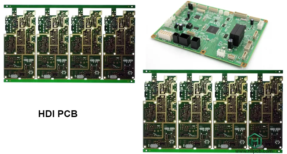
At HILPCB, we manufacture HDI printed circuit boards as part of our comprehensive PCB services, handling everything from rigid-flex hybrid designs to standard FR4 constructions. Our integrated facility provides design support, fabrication, and complete assembly capabilities, helping engineers and manufacturers bring complex electronics to market efficiently.
Understanding Cost Drivers in HDI Printed Circuit Board Production
Layer Count and Sequential Lamination Complexity
Unlike conventional boards manufactured through single lamination cycles, HDI printed circuit boards build up layers progressively—adding thin dielectric layers and copper foil in multiple press operations. Each lamination cycle adds cost.
Build-Up Structure Economics:
1+N+1 HDI structures (one build-up layer each side) represent the most economical approach, adding roughly 35-50% to equivalent standard multilayer board costs. This configuration suits most moderate-density applications including smart home devices, portable instruments, and automotive control modules.
2+N+2 structures with two build-up layers per side enable higher routing density through stacked or staggered microvias. Manufacturing cost increases approximately 70-90% versus conventional boards—still economical when the alternative requires adding 2-4 more signal layers using standard technology.
Advanced any-layer HDI where microvias connect arbitrary layer pairs provides maximum density but costs 2-3x conventional boards. We typically recommend this only when space constraints are absolute or when avoiding additional layers justifies the premium.
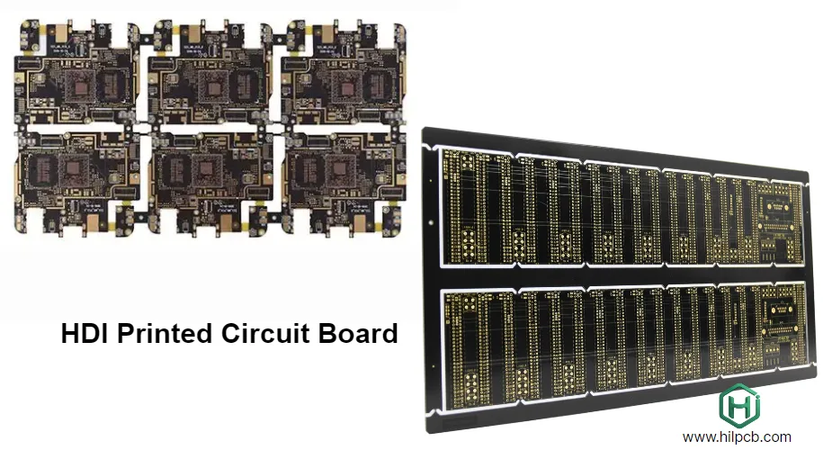
Our multilayer PCB capabilities span 4-32 layers, allowing us to optimize the balance between layer count and HDI complexity for your specific application.
Microvia Drilling and Via Processing Costs
Laser drilling accounts for 15-25% of total HDI printed circuit board costs versus mechanical drilling representing only 5-10% of standard PCB costs. However, the comparison requires context.
Via Cost Analysis:
Mechanical drilling costs scale primarily with hole count—drilling 1000 holes costs roughly 10x more than drilling 100 holes. Laser drilling costs correlate more with panel area than via count. Within reason, adding microvias has minimal cost impact once laser systems are programmed and aligned.
This cost structure makes HDI economical for very high via density designs. When microvia counts exceed several thousand per board, HDI may actually cost less than attempting equivalent density with mechanical drilling—even ignoring HDI's routing density advantages.
Via plating processes cost similar between standard and HDI boards, though HDI's thinner copper and smaller features demand tighter process control. We've optimized our electroless and electrolytic copper plating specifically for reliable microvia fill on high-density interconnect boards.
Material Selection Impact on Pricing
HDI printed circuit boards use specialized materials formulated for sequential lamination and fine feature processing.
Material Cost Factors:
Standard FR-4 works for many HDI applications and costs essentially the same as in conventional boards. However, HDI often benefits from modified FR-4 formulations with lower resin flow and tighter dimensional stability—adding 10-15% material cost.
High-performance materials like halogen-free laminates or polyimide substrates increase costs more substantially—typically 40-80% material premiums. These choices make sense when environmental regulations mandate halogen-free construction or when thermal performance justifies polyimide.
RCC (resin-coated copper) foils used in HDI build-up layers cost more than standard copper foil but enable the thin dielectrics HDI requires. This represents a necessary cost component rather than an optional upgrade.
Optimizing Design for Cost-Effective HDI Manufacturing
Via Design Strategy for Cost Reduction
How you structure interconnections dramatically affects manufacturing complexity and cost.
Cost-Conscious Via Approaches:
Use blind microvias between adjacent layers only—avoiding stacked or buried vias when possible. This simplifies processing and improves yield, reducing per-board costs by 20-30% versus complex via stacking schemes.
When stacking proves necessary, limit stack depth to 2-3 layers maximum. Deeper stacks require additional lamination cycles and reliability concerns demand more rigorous testing, both increasing costs.
Standardize microvia sizes rather than mixing multiple diameters. Using consistent 0.10mm or 0.15mm microvias throughout simplifies laser programming and reduces setup time versus boards requiring frequent diameter changes.
Our engineering team reviews every design for via optimization opportunities during DFM analysis. Often simple via placement adjustments reduce manufacturing complexity without affecting electrical performance—savings we pass directly to customers.
Panel Utilization and Array Configuration
How boards fit within production panel sizes significantly impacts per-unit pricing—especially for smaller designs.
Panelization Optimization:
Standard panel sizes include 12"x18", 16"x18", and 18"x24". Designs should array efficiently within these dimensions to minimize material waste. A 100mm x 100mm board fits 12 pieces per 18"x18" panel, but a 110mm x 110mm board only fits 8 pieces—increasing per-board cost 50% despite being only 10mm larger.
We help customers optimize board dimensions during initial quoting. Sometimes slight size adjustments dramatically improve panel utilization—and we'll identify these opportunities before finalizing your design.
Breakaway tabs and routing channels consume panel space but represent essential fabrication costs. Our standard allowances enable reliable board separation without damage. Custom tooling can minimize these areas for very high-volume production, amortizing tooling costs across large quantities.
Layer Stack-Up Simplification
HDI printed circuit boards offer opportunities to reduce total layer count versus achieving equivalent density with conventional technology—potentially offsetting HDI's higher per-layer costs.
Stack-Up Cost Optimization:
An 8-layer conventional board might accomplish the same routing density as a 6-layer HDI board. Although HDI costs more per layer, two fewer layers often compensate—resulting in comparable or lower total cost while offering thinner profile and better electrical performance.
This analysis requires detailed routing assessment. Submit your current design or routing requirements for feasibility evaluation. Our engineers will model both conventional and HDI approaches, providing accurate cost and performance comparisons.
Power distribution often drives layer count in conventional designs. HDI's ability to route traces between closely-spaced microvia pads enables denser power distribution with fewer dedicated layers. We've helped customers eliminate 2-4 power/ground layers through HDI conversion—dramatic cost savings.
Fast-Turn HDI Printed Circuit Board Manufacturing
Prototype and Small Batch Quick-Turn Services
Speed to market matters—especially for competitive consumer electronics and fast-moving IoT products. Our quick-turn HDI services accelerate development cycles.
Accelerated Manufacturing Options:
Standard HDI delivery takes 15-18 working days from order to shipment. This covers design review, material procurement, multi-stage fabrication, testing, and quality inspection. For most projects, this timeline suits development schedules well.
Express HDI service delivers in 10-12 days for urgent requirements. We prioritize express orders through our production flow while maintaining full quality standards—no shortcuts that compromise reliability. Express service typically adds 30-40% to standard pricing but proves worthwhile when time-to-market is critical.
Ultra-rapid 7-day HDI serves true emergencies where every day counts. This requires dedicated production scheduling and possible material expediting. While expensive—often 80-100% premium over standard pricing—it has saved numerous product launches from expensive delays.
Our small batch assembly services complement quick-turn fabrication, providing complete assembled boards in the same accelerated timeframes when needed.
Design Review and DFM Optimization Speed
Quick turnaround requires efficient design verification to avoid revision cycles that consume the time savings.
Expedited Engineering Review:
Standard DFM review delivers within 24 hours of file submission. Our engineering team examines manufacturability, identifies potential yield issues, and suggests optimizations—all documented in comprehensive review reports.
Same-day DFM review is available for express orders, providing feedback within 4-6 hours during business hours. This enables rapid iteration when refining designs under tight schedules.
Use our online Gerber viewer and 3D visualization tool for immediate preliminary verification before formal DFM submission. These tools catch obvious errors quickly, though they don't replace comprehensive manufacturing review.
Production Ramp from Prototype to Volume
Smooth transition from prototypes through pilot production to high-volume manufacturing prevents expensive surprises and delays.
Staged Production Approach:
Initial prototypes validate design feasibility and catch functional issues. We typically recommend 5-10 pieces for first-article validation regardless of ultimate volume requirements.
Pilot production runs of 25-100 pieces verify manufacturing repeatability and test assembly processes before committing to full production tooling. This stage often reveals opportunities to optimize manufacturing yield or reduce costs—lessons that pay dividends at volume.
Volume production handles quantities from hundreds to millions of pieces. Our high-volume assembly lines scale efficiently while maintaining the same quality standards as prototype builds. Per-unit costs typically decrease 40-60% when transitioning from prototypes to 1000+ piece production runs.
Quality Assurance in Cost-Effective HDI Production
Process Control Without Excessive Testing Costs
Balancing thorough quality verification with cost control requires smart process monitoring and strategic testing.
Efficient Quality Approach:
In-process monitoring catches issues early when correction costs minimal time and materials. Automated optical inspection after each critical process step—laser drilling, imaging, etching, plating—prevents defects from propagating through subsequent operations.
Statistical process control tracks key parameters across production lots. Rather than testing every parameter on every board, we monitor trends and flag any drift before it causes quality issues. This provides equivalent or better assurance than 100% testing while reducing inspection costs.
Electrical testing strategy depends on production volume and application criticality. Prototypes receive 100% flying probe testing—flexible and economical for small quantities. Production runs transition to dedicated test fixtures that provide faster testing, amortizing fixture investment across larger quantities.
Reliability Qualification for High-Volume Production
Production quantities justify investment in comprehensive reliability testing that prototype budgets cannot support.
Validation Testing Programs:
Thermal cycling validation subjects sample boards to temperature extremes (-40°C to +125°C) for 500-1000 cycles while monitoring electrical continuity. This accelerated stress testing simulates years of operational thermal exposure, revealing latent failures before field deployment.
Cross-sectional microsection analysis verifies internal structure quality through destructive examination of coupon samples. We examine microvia fill quality, layer bonding, and copper plating uniformness—aspects invisible during electrical testing.
This reliability data accompanies production lots for applications requiring documented quality assurance. Medical device manufacturers and automotive suppliers particularly value this validation for regulatory compliance and warranty risk management.
Cost-Effective Certification and Compliance
Certifications add cost but may be mandatory for certain markets or applications while providing competitive advantages.
Strategic Certification Approach:
ISO 9001:2015 certification demonstrates quality management system maturity and costs relatively little to maintain once implemented. We include this at no extra charge—it's standard for professional manufacturing.
UL recognition for flame rating and electrical safety matters for products sold in North America. Material certification costs add 5-10% to production costs but may be legally required depending on end application.
ITAR registration for military/defense work requires significant compliance overhead. We support ITAR projects including specialized substrates but recommend this only when end-use truly requires it—costs increase 20-30% beyond technical complexity alone.
Working with HILPCB for HDI Printed Circuit Board Projects
For every HDI printed circuit board project, efficiency, flexibility, and accountability are just as important as precision manufacturing. HILPCB simplifies complex PCB programs through fast quoting, scalable production, and complete turnkey service—helping customers move from prototype to mass production seamlessly.
Key elements of our service approach include:
- Instant online quoting that provides transparent pricing within minutes for standard HDI configurations, with custom quotes delivered within 24 hours
- Flexible order volumes supporting everything from single prototypes to large-scale production, without unnecessary minimums or extra tooling costs
- Streamlined turnkey manufacturing combining fabrication, component sourcing, SMT assembly, and testing under one roof for faster, more reliable delivery
- Automated BOM verification using our BOM viewer tool to identify component issues early and prevent sourcing delays
- Dedicated engineering support ensuring design optimization, DFM review, and process consistency across every build
By consolidating PCB fabrication and assembly, we reduce coordination overhead and lead time, while maintaining a single point of responsibility for quality and performance. Our integrated workflow allows you to launch HDI printed circuit board designs faster—with predictable quality, lower total cost, and dependable supply continuity for every stage of production.