For electronics operating in extreme environments, High-Temperature Co-Fired Ceramic (HTCC) PCB technology provides the ultimate solution for durability and thermal stability. At HILPCB, we are experts in end-to-end HTCC PCB manufacturing and assembly, offering turnkey support from substrate engineering to final component integration.
Our process-driven approach supports the most demanding applications in aerospace, automotive, medical, and power electronics, where thermal reliability, hermeticity, and electrical integrity are non-negotiable. By leveraging advanced ceramic co-firing, metallization, and packaging technologies, we empower engineers to create electronics that perform flawlessly under the harshest thermal and mechanical stress.
Understanding HTCC PCB Technology
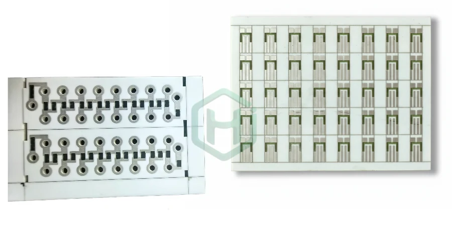
HTCC technology involves laminating multiple layers of high-purity alumina (Al₂O₃) or aluminum nitride (AlN) ceramic "green" tapes. Conductive traces made from tungsten (W) or molybdenum-manganese (Mo-Mn) paste are screen-printed onto each layer. The stacked layers are then co-fired in a controlled atmosphere at over 1,600°C. This process sinters the materials into a monolithic, hermetically sealed structure with exceptional mechanical strength and dielectric properties.
Unlike other Ceramic PCB Manufacturing methods, HTCC embeds the metallization within the ceramic layers before firing. This creates a fully integrated, gas-tight assembly ideal for high-voltage power modules, implantable medical devices, and avionics systems that must withstand severe thermal cycling.
Core Advantages of HTCC:
- Exceptional Thermal Stability: Capable of continuous operation at temperatures up to 500°C with minimal material degradation.
- High Thermal Conductivity: Efficiently dissipates heat with values up to 180 W/m·K using AlN.
- Inherent Hermeticity: The dense, monolithic structure provides a perfect seal against moisture and gas ingress.
- Superior Electrical Insulation: Offers high dielectric strength (>15 kV/mm) for high-voltage applications.
- Matched CTE: The coefficient of thermal expansion (CTE) closely matches that of silicon, minimizing stress on attached semiconductor devices.
These properties make HTCC indispensable in environments where conventional FR-4 or other organic laminates would fail, ensuring unmatched long-term reliability.
HTCC vs. LTCC and Thin Film PCB: A Comparison
While all are ceramic-based, HTCC, LTCC (Low-Temperature Co-Fired Ceramic), and Thin Film PCB technologies serve distinct performance needs.
| Feature | HTCC | LTCC | Thin Film PCB |
|---|---|---|---|
| Firing Temperature | >1,600°C | ~850°C | N/A (Vacuum Deposition) |
| Conductor Material | Tungsten (W), Molybdenum (Mo) | Silver (Ag), Gold (Au) | Gold (Au), Copper (Cu), Platinum (Pt) |
| Mechanical Robustness | Extremely High | High | Substrate Dependent |
| Hermeticity | Excellent (Inherent) | Good (Requires Sealing) | Excellent (Substrate Dependent) |
| Line Precision | 100–150 µm | 50–100 µm | <10 µm |
| Max Operating Temp. | >500°C | ~250°C | Typically <200°C |
In essence, HTCC excels in power handling and high-temperature endurance, LTCC is optimized for high-frequency RF modules, and Thin Film PCB delivers ultimate precision for microwave and optical circuits. HILPCB often integrates these technologies, for instance, by combining HTCC power stages with thin film signal layers to create advanced hybrid ceramic assemblies.
Material and Process Characteristics
The performance of an HTCC circuit is defined by the precise synergy between its materials and the co-firing process. HILPCB meticulously controls each parameter to ensure consistent, high-quality results.
Ceramic Substrates
- Alumina (Al₂O₃, 92–96%): The industry standard, offering a robust balance of dielectric strength, mechanical integrity, and cost-effectiveness.
- Aluminum Nitride (AlN): The premier choice for thermal management, essential for cooling high-power semiconductors and RF amplifiers.
- Zirconia-Toughened Alumina (ZTA): Provides enhanced mechanical toughness for systems exposed to high shock and vibration.
Metallization Systems
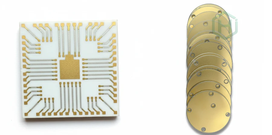
- Tungsten (W): Used for internal traces and vias due to its high melting point and stability during co-firing.
- Molybdenum-Manganese (Mo-Mn): Often used for external metallization, providing a strong bond that is compatible with post-fire Ni/Au plating for soldering and wire bonding.
After firing, all exposed metal surfaces are plated to ensure reliable electrical connections during the Ceramic PCB Assembly stage.
The Co-Firing Process
Each ceramic layer is screen-printed, vias are punched for interlayer connections, and the layers are laminated under precisely controlled pressure and heat. This alignment (typically ±10 µm) is critical. The subsequent co-firing in a reducing atmosphere fuses all layers into a single, dense ceramic block, guaranteeing dimensional stability and electrical isolation across even the most complex multilayer structures. This precision enables the integration of embedded passive components and high-current vias essential for miniaturized, high-power designs.
Reliability in High-Temperature and High-Power Applications
HTCC PCBs are engineered to outperform conventional substrates under extreme thermal, electrical, and environmental stress. Our HTCC solutions provide predictable, stable performance for mission-critical systems.
Thermal and Mechanical Endurance
- Operating Range: –55°C to +500°C
- Power Cycling Durability: Proven to withstand >100,000 thermal cycles.
- Thermal Conductivity: 24 W/m·K (Alumina) to 180 W/m·K (AlN).
- CTE Matching: A CTE of 7–9 ppm/°C closely matches silicon, minimizing mechanical stress on components.
Electrical and Environmental Stability
- Stable Dielectric Constant: Remains consistent (9.5–10.2 for Alumina) well into millimeter-wave frequencies.
- Certified Hermeticity: Ensures helium leak rates as low as 10⁻⁹ atm·cc/s.
- Reliable Surface Finishes: Ni/Au, Ag, or Pt finishes support robust wire bonding and soldering for long-term interconnect reliability.
Proven Application Examples
- Aerospace & Defense: T/R modules for phased-array radar, inertial navigation sensors, and power distribution units.
- Automotive: Power inverters for electric drives, high-temperature sensor housings, and battery management systems.
- Medical: Implantable neurostimulators, diagnostic tool heads, and modules for sterilizable surgical equipment.
- Industrial Power: High-voltage DC-DC converters, laser drivers, and renewable energy modules.
HILPCB's Advanced Fabrication and Quality Assurance
HILPCB integrates engineering design, ceramic processing, and assembly verification into a seamless workflow, ensuring high yields and repeatable quality for every project.
Engineering and Design Support
- Thermal & Signal Integrity Modeling: 2D/3D simulation to optimize performance.
- Multilayer Stack-Up Design: Expert guidance on architectures up to 30+ layers.
- Hybrid Integration: Combining HTCC, LTCC, and other Ceramic PCB Manufacturer processes for optimal system design.
Key Fabrication Parameters
- Min. Line/Space: 100 µm / 100 µm
- Min. Via Diameter: 75 µm
- Layer Count: 2 to 30+
- Substrate Thickness: 0.25 mm to 2.0 mm
- Surface Finishes: ENIG (Ni/Au), ENEPIG, Silver (Ag), Platinum (Pt)
Inspection and Reliability Testing
All HTCC circuits undergo rigorous qualification:
- Cross-section analysis to verify metallization bonding.
- Helium leak testing to confirm hermeticity.
- Dielectric breakdown and insulation resistance testing.
- Environmental stress screening (thermal shock, vibration).
- AOI and X-ray inspection to ensure assembly readiness.
Our processes are managed by Statistical Process Control (SPC) and are certified under ISO 9001, IATF 16949, and AS9100, ensuring full compliance with the strictest industry requirements.
Partner with HILPCB Factory for Reliable HTCC PCB Manufacturing
At HILPCB Factory, we combine advanced ceramic processing with precision electronic manufacturing to deliver high-reliability HTCC PCBs for harsh and high-performance environments. Our expertise covers every stage—from green tape preparation, metallization, and co-firing to final assembly and testing—ensuring consistent quality and long-term durability.
We provide end-to-end service that integrates HTCC fabrication, Ceramic PCB Assembly, and reliability validation under one roof. Each build undergoes electrical, thermal, and mechanical testing to guarantee performance stability across wide temperature and power ranges.
Why Choose HILPCB
- Complete Manufacturing Integration: In-house co-firing, metallization, laser processing, and assembly for total process control.
- Engineering Collaboration: DFM/DFA review and material optimization for high-frequency, power, and medical designs.
- Scalable Production: Rapid prototype delivery and stable quality in large-scale production.
- Certified Quality: ISO 9001, IATF 16949, and AS9100 compliance ensuring aerospace- and automotive-grade reliability.
Our HTCC solutions serve industries including aerospace, automotive power electronics, medical devices, and industrial energy systems, where heat resistance, hermetic sealing, and electrical precision are essential.
By combining ceramic technology with modern PCB assembly and testing capabilities, HILPCB Factory ensures your HTCC boards perform reliably in mission-critical environments—from satellites and radar systems to EV inverters and implantable medical sensors.