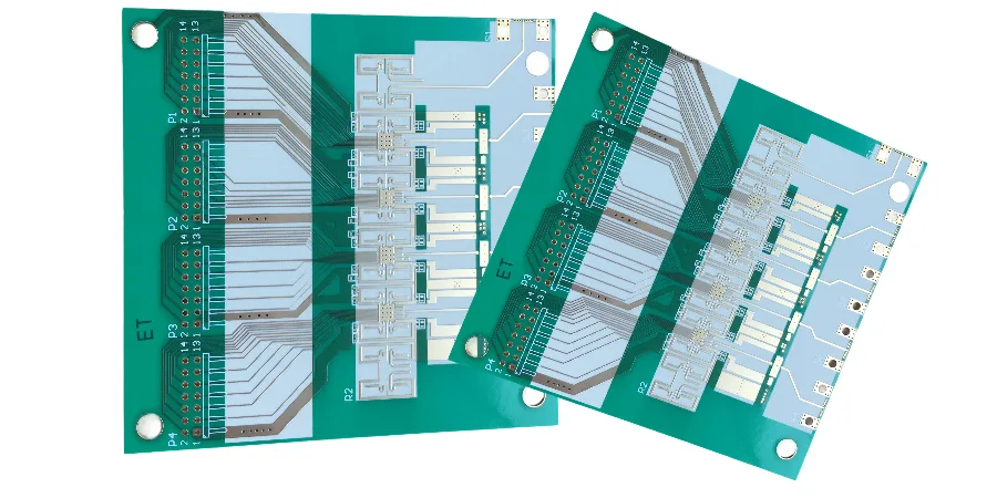
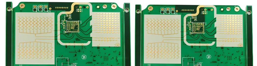
Highleap PCB Factory (HILPCB) specializes in manufacturing advanced hybrid circuit boards that strategically combine different substrate materials within a single PCB stackup. Our hybrid PCB solutions optimize electrical performance for high-frequency signals while maintaining cost-effectiveness through selective use of premium materials exactly where needed, delivering superior value for telecommunications, aerospace, and high-speed digital applications.
Advanced Material Integration and Electrical Performance Optimization
Hybrid circuit board technology represents a sophisticated approach to PCB design where different dielectric materials are strategically combined within a single stackup to optimize electrical performance while controlling costs. The fundamental principle involves using high-performance materials like PTFE, Rogers, or ceramic-filled laminates only in critical signal paths, while employing standard FR-4 PCB materials for power, ground, and low-speed digital layers.
Critical Design Parameters for Material Selection
The selection of materials in hybrid PCBs requires careful analysis of multiple parameters:
| Parameter | FR-4 (Standard) | Rogers RO4003C | Rogers RO4350B | PTFE/Teflon |
|---|---|---|---|---|
| Dielectric Constant (Dk) @ 10GHz | 4.2-4.5 | 3.38 ± 0.05 | 3.48 ± 0.05 | 2.1-2.3 |
| Dissipation Factor (Df) @ 10GHz | 0.020-0.025 | 0.0027 | 0.0037 | 0.0002-0.0008 |
| Thermal Conductivity (W/m·K) | 0.3-0.4 | 0.71 | 0.69 | 0.2-0.3 |
| CTE-Z (ppm/°C) | 70-80 | 46 | 32 | 150-200 |
| Tg (°C) | 130-180 | >280 | >280 | 327 |
| Moisture Absorption (%) | 0.15-0.30 | 0.04 | 0.04 | <0.01 |
Signal Integrity Considerations
For high-speed digital applications exceeding 10 Gbps, the hybrid approach enables controlled impedance traces with minimal loss. Critical high-speed differential pairs route through low-loss materials (Df < 0.004), while power delivery networks utilize standard FR-4. This selective approach maintains signal integrity where needed while reducing overall board cost by 30-50%.
The transition between materials requires careful impedance matching to minimize reflections. Our design guidelines specify:
- Gradual trace width transitions over 3-5 times the trace width
- Via stub elimination through back-drilling in thick boards
- Matched dielectric thickness to maintain consistent impedance
- Ground plane continuity across material boundaries
Advanced hybrid designs incorporate thermally conductive materials in specific zones. For power amplifier applications, we integrate materials like Arlon 92ML (thermal conductivity 2.0 W/m·K) or aluminum-backed substrates beneath high-dissipation components, while maintaining RF performance through careful stackup design. This localized thermal management approach eliminates the need for expensive thermal vias throughout the entire board.
Manufacturing Process Control for Dissimilar Material Bonding
The manufacturing of hybrid circuit boards presents unique challenges in bonding materials with different physical and chemical properties. Our specialized processes ensure reliable adhesion while maintaining the integrity of each material system:
Pre-lamination Material Preparation
Different substrate materials require specific surface treatments before lamination:
- PTFE surfaces: Sodium etching or plasma treatment to enhance adhesion
- Rogers materials: Controlled oxide formation for optimal bonding
- FR-4: Standard brown oxide or alternative oxide processes
- Ceramic-filled laminates: Specialized coupling agents for interface stability
Optimized Lamination Profiles
Each material combination requires a unique lamination profile accounting for:
- Different resin flow characteristics (PTFE: minimal flow vs. FR-4: 15-25% flow)
- Varied cure temperatures (FR-4: 175-185°C vs. high-Tg materials: 200-220°C)
- Mismatched thermal expansion during heating (CTE management)
- Pressure optimization to prevent crushing of low-density materials
Our advanced hydraulic presses feature:
- Independent heating zones with ±2°C control
- Programmable pressure profiles from 200-500 PSI
- Cooling rate control to minimize stress
- In-situ thickness monitoring for process verification
Critical Process Parameters
Sequential build-up processes for complex hybrid stackups:
- Core preparation with matched CTE materials
- First lamination cycle for compatible material groups
- Intermediate inspection and surface preparation
- Second lamination with transition prepregs
- Final pressing with optimized cool-down profile
The use of specialized bonding films with intermediate properties helps bridge the gap between dissimilar materials, preventing delamination during thermal cycling.
RF and Microwave Performance in Hybrid Structures
Hybrid PCBs excel in high-frequency PCB applications where selective use of low-loss materials dramatically improves performance:
Insertion Loss Optimization
For a typical 77 GHz automotive radar application:
- Signal path through 5 mil Rogers RO3003: 0.8 dB/inch loss
- Power/digital through FR-4: Acceptable for DC-1 GHz signals
- Total insertion loss reduction: 60% versus all-FR-4 design
- Cost savings: 45% versus all-Rogers construction
Phase Stability and Temperature Performance
Critical for phased array antennas and beamforming networks:
- Temperature coefficient of Dk for PTFE: 0 to -12 ppm/°C
- FR-4 temperature coefficient: -70 to -150 ppm/°C
- Hybrid approach maintains ±2° phase stability over -40 to +85°C
- Selective material use in delay lines and phase shifters
Harmonic Control and Intermodulation
The non-linear properties of different dielectrics affect harmonic generation:
- PTFE exhibits lowest third-order intercept point degradation
- Strategic placement reduces PIM (Passive Intermodulation) by 15-20 dB
- Critical for cellular base station and satellite communication applications
Testing and Reliability Validation for Hybrid PCBs
Comprehensive testing ensures hybrid circuit boards meet stringent reliability requirements:
Material Interface Testing
- Cross-sectional analysis at 200-500X magnification
- Dye penetrant testing for micro-delamination detection
- Acoustic microscopy (C-SAM) for void detection
- Peel strength testing exceeding 6 lb/inch per IPC-TM-650
Electrical Characterization
- Vector Network Analyzer testing to 110 GHz
- TDR impedance profiling with 35ps rise time
- Insertion loss measurement per IPC-TM-650 2.5.5.12
- Crosstalk evaluation at material transitions
Environmental Stress Testing
- Thermal cycling: -65°C to +150°C, 1000 cycles minimum
- HAST (Highly Accelerated Stress Test): 130°C/85% RH/96 hours
- Vibration testing per MIL-STD-883 Method 2007
- Thermal shock: -55°C to +125°C, 15-minute dwell
Long-term Reliability Monitoring
- Insulation resistance after moisture exposure
- CAF (Conductive Anodic Filament) resistance testing
- Interconnect stress testing for 2000 hours
- Field failure analysis and corrective action database
Complete Hybrid PCB Manufacturing Solutions
Hybrid circuit boards are designed to balance performance with cost—by selectively using high-end materials like PTFE or ceramic only where electrical or thermal demands require them, while employing standard materials like FR-4 elsewhere. This strategic approach allows engineers to achieve excellent signal integrity, thermal control, and reliability—without the expense of building the entire board from premium substrates.
At HILPCB, we specialize in manufacturing hybrid PCBs of any complexity, helping our customers reduce material costs by up to 50% without compromising functionality. Whether your design integrates RF layers, high-voltage cores, or thermally enhanced zones, we support full-stack customization across diverse industries including 5G infrastructure, aerospace, automotive, medical, and industrial control.
With deep expertise in materials, lamination strategies, and mixed-technology integration, we deliver complete hybrid PCB solutions tailored to your technical goals and budget constraints—ensuring optimal performance, manufacturability, and value.
FAQ
What cost savings can hybrid PCBs provide versus all-PTFE designs?
Hybrid circuit boards typically reduce material costs by 40-60% compared to using PTFE throughout the stackup. For a 10-layer board with 2 RF layers, material cost savings range from $80-150 per panel depending on size. Additional savings come from easier processing of FR-4 layers, reducing overall manufacturing costs by 25-35%.
How do you ensure reliable bonding between different materials?
We utilize specialized thermoplastic bonding films like Rogers 2929 or Taconic FastRise™ prepregs designed for dissimilar material adhesion. These materials feature intermediate CTE values and optimized flow characteristics. Combined with sequential lamination and precise temperature control, we achieve peel strengths exceeding 8 lb/inch at material interfaces.
What are the minimum order quantities for hybrid PCB prototypes?
No minimum order quantity exists for hybrid PCB prototypes. We regularly produce single prototype boards for proof-of-concept testing. Standard lead times are 10-15 days for hybrid designs, with expedited 7-day service available for simpler stackups.
Can hybrid boards combine rigid and flex materials?
Yes, rigid-flex PCB designs can incorporate hybrid material stackups. For example, combining Rogers materials in rigid sections with polyimide flex layers. Critical considerations include CTE matching at transition zones and specialized adhesives accommodating different material properties.
How do you handle impedance control at material transitions?
We employ 3D electromagnetic field solvers to model impedance discontinuities at material boundaries. Design adjustments include trace width compensation, reference plane modifications, and gradual dielectric transitions. Typical impedance control achieves ±5% tolerance even across material transitions.
What file formats do you accept for hybrid PCB designs?
We accept all standard CAD formats including Gerber RS-274X, ODB++, and native files from Altium, Cadence, and Mentor Graphics. Our impedance calculator helps verify controlled impedance requirements for different material combinations. Provide detailed stackup drawings specifying material placement for optimal quoting accuracy.