Highleap PCB Factory (HILPCB) specializes in manufacturing sophisticated LTCC PCBs that enable breakthrough performance in RF/microwave systems, automotive electronics, and high-density packaging. Our low temperature co-fired ceramic technology delivers unmatched integration density, embedded passive components, and superior high-frequency characteristics for demanding applications where traditional PCB technologies reach their limits.
Advanced LTCC Technology and Material Systems
Low Temperature Co-fired Ceramic technology represents a paradigm shift in ceramic PCB manufacturing, enabling complex 3D architectures impossible with traditional substrates. The fundamental advantage of LTCC lies in its unique glass-ceramic composition that allows co-firing with high-conductivity metals at temperatures below 900°C, preserving the exceptional electrical and mechanical properties while enabling cost-effective precious metal conductor systems.
The material science behind LTCC involves carefully engineered glass-ceramic composites that crystallize during firing to create a dense, hermetic structure. This process results in substrates with dielectric constants tailorable from 4.0 to 9.0, enabling impedance matching for various applications. The low loss tangent of 0.001-0.003 at 10 GHz ensures minimal signal attenuation, critical for millimeter-wave applications. With thermal conductivity ranging from 2-5 W/m·K and CTE precisely matched to silicon at 4.0-7.0 ppm/K, LTCC substrates provide reliable interconnections in thermally demanding environments.
Design Capabilities and 3D Integration Features
Embedded Passive Components
- Printed resistors: 10Ω/□ to 1MΩ/□ with ±10% tolerance
- Integrated capacitors: 0.1pF to 10nF using high-K dielectrics
- Embedded inductors: Spiral and helical designs to 100nH
- Filters and baluns: Complete RF circuits within substrate
- Thermal management: Integrated heat spreaders and vias
Advanced Structural Features
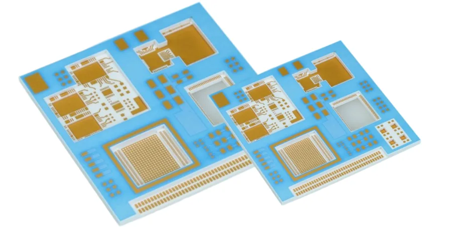
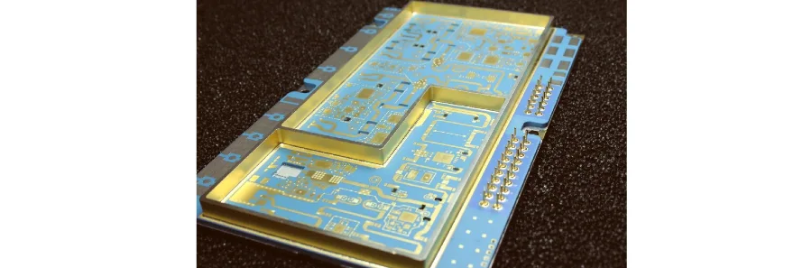
- Hermetic cavities for MEMS and SAW devices
- Microfluidic channels for cooling or sensing
- Stepped cavities for multi-chip modules
- Edge metallization for shielding
- Integrated antennas with controlled radiation patterns
The three-dimensional integration capabilities of LTCC technology far exceed traditional PCB manufacturing methods. Complex cavities can be formed within the substrate for component protection or to create controlled environments for sensitive devices. Microfluidic channels enable innovative cooling solutions or lab-on-chip applications. The ability to create different dielectric constants within a single substrate through material selection enables integrated antenna designs with superior performance compared to surface-mounted alternatives.
Manufacturing Process Excellence for LTCC PCBs
HILPCB's state-of-the-art LTCC manufacturing facility combines precision equipment with rigorous process controls to deliver consistent quality. Our green tape processing begins with incoming material inspection verifying dielectric properties and dimensional stability. Automated optical inspection after each printing step ensures pattern integrity, while advanced lamination systems apply uniform pressure preventing layer shifting or delamination.
The critical firing process utilizes multi-zone furnaces with ±2°C temperature uniformity across the heating profile. Constrained sintering technology controls X-Y shrinkage to ±0.2%, enabling accurate post-fire dimensions essential for fine-pitch component assembly. Post-fire processes include laser trimming for passive component adjustment, edge metallization for EMI shielding, and surface treatments optimizing solderability or wire bonding.
Quality verification encompasses electrical testing using network analyzers up to 67 GHz, confirming impedance control and insertion loss specifications. X-ray inspection reveals internal defects such as delamination or via misalignment. For hermetic packages, helium leak testing ensures seal integrity meeting MIL-STD-883 requirements. Environmental testing including thermal cycling, humidity exposure, and mechanical shock validates long-term reliability for demanding applications.
Application Solutions and Industry Implementation
LTCC PCBs enable breakthrough performance across diverse industries:
5G and Millimeter-Wave Communications
- Antenna-in-package (AiP) for 28/39/77 GHz bands
- Beamforming modules with integrated phase shifters
- Front-end modules with embedded filters
- Power amplifier substrates with thermal vias
- mmWave radar for automotive ADAS
Automotive Electronics
- Engine control modules surviving 150°C continuous operation
- Pressure sensors with integrated signal conditioning
- Airbag firing circuits with high reliability
- LED driver modules for adaptive headlights
- Battery management systems for EVs
Aerospace and Defense
- Radar T/R modules with hermetic packaging
- Satellite communication subsystems
- Missile guidance electronics
- Avionics modules meeting DO-160 standards
- Space-qualified packages for extreme environments
Medical and Scientific Instrumentation
- Implantable device packages with biocompatible coatings
- High-frequency ultrasound transducers
- Lab-on-chip devices with microfluidics
- Precision sensor modules
- MRI-compatible electronics
Our turnkey assembly services include die attachment, wire bonding, and hermetic sealing, delivering complete LTCC-based modules ready for system integration with specialized processes for medical applications including biocompatible coatings and sterilization-compatible packaging.
Complete LTCC Solutions from Design to Delivery
Partnering with HILPCB provides comprehensive support throughout your LTCC product development journey. Our experienced engineering team collaborates from concept through production, offering design optimization suggestions that improve manufacturability while maintaining performance objectives. We maintain extensive libraries of proven embedded component designs and substrate configurations, accelerating development schedules and ensuring first-pass success.
Our production capabilities scale seamlessly from prototype quantities to large-volume assembly, with dedicated LTCC manufacturing lines ensuring consistent quality. Advanced scheduling systems optimize production flow, delivering prototypes in 15-20 days while maintaining competitive pricing for volume orders. Established relationships with material suppliers ensure consistent availability of specialized LTCC tapes and conductor pastes.
Global logistics expertise ensures safe delivery of delicate ceramic substrates worldwide. Custom packaging solutions protect against mechanical damage during shipment while moisture barrier packaging prevents atmospheric contamination. Multiple payment options including wire transfer, PayPal, and letter of credit accommodate diverse customer requirements. Our commitment extends beyond delivery with ongoing technical support, failure analysis capabilities, and continuous improvement initiatives enhancing product quality and reducing costs.
Frequently Asked Questions
What advantages does LTCC offer over traditional PCB technologies?
LTCC enables true 3D integration with embedded components, cavities, and channels impossible in organic PCBs. The hermetic ceramic structure provides zero moisture absorption, exceptional dimensional stability, and operation beyond 200°C. High-frequency performance exceeds any organic substrate with lower loss and better phase stability.
What are typical tolerances for LTCC manufacturing?
Dimensional tolerances achieve ±0.2% post-firing with constrained sintering. Feature sizes include 100μm minimum line width/spacing, 150μm minimum via diameter, and ±12.5μm layer-to-layer registration. Passive component values maintain ±10% tolerance with laser trimming available for ±5% or tighter specifications.
Can LTCC substrates integrate with standard SMT assembly?
Yes, LTCC substrates are fully compatible with standard SMT assembly processes. Post-fired metallization provides solderable surfaces for component attachment. The constrained sintering technology ensures accurate component placement. Special handling accounts for ceramic brittleness during assembly.
What design software supports LTCC development?
Major EDA tools including Cadence, Mentor Graphics, Ansys HFSS, and ADS support LTCC design with appropriate material libraries. We provide design rules and stackup information compatible with standard tools. Our engineering team assists with 3D model creation for electromagnetic and thermal simulation.
How do LTCC costs compare to other packaging technologies?
LTCC typically costs 2-5x more than organic substrates but often reduces total system cost through integration. Embedding passive components eliminates discrete parts and assembly steps. The ability to combine multiple functions in one hermetic package provides significant value for high-reliability applications requiring high-frequency PCB performance.