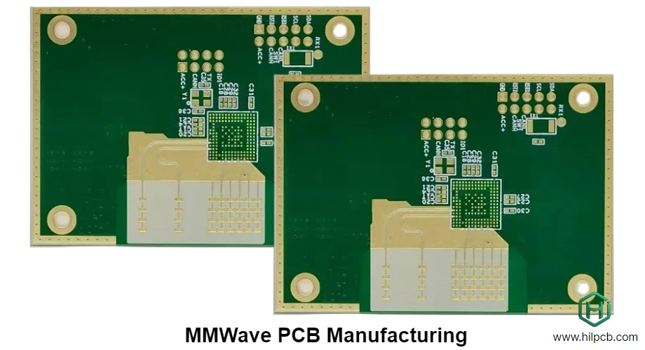
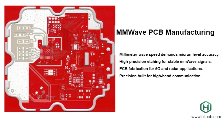
As wireless communication technology advances, MMWave PCBs (millimeter-wave PCBs) have become the backbone of high-speed applications such as 5G, automotive radar, and satellite communication. At HILPCB, we offer expert MMWave PCB manufacturing services designed to meet the specific demands of these high-frequency systems.
Our services encompass every step from design to mass production, ensuring your PCB performs flawlessly at frequencies from 30GHz to 77GHz. In this article, we’ll explore the critical considerations in MMWave PCB design and manufacturing, from material selection to thermal management, and provide solutions to common challenges.
Key Factors in MMWave PCB Manufacturing
MMWave PCBs present unique challenges due to the high frequencies involved. Successful MMWave PCB manufacturing requires precision in design, material selection, and fabrication to ensure that performance is not compromised.
1. Material Selection for MMWave PCBs
Choosing the right material is crucial for MMWave PCB performance, as it directly affects the signal integrity, loss, and overall efficiency of the system.
- High-performance materials like RO4003C and RO5880 are ideal for frequencies above 30GHz, ensuring low-loss transmission and stability.
- PTFE-based substrates provide the lowest loss for high-frequency applications, making them suitable for 5G and other advanced wireless technologies.
Solution: For 5G and high-frequency systems, select low-loss materials such as RO4003C for up to 40GHz and RO5880 for frequencies above 20GHz. This minimizes signal degradation and ensures reliable communication.
2. Design Considerations for MMWave PCB Layout
Effective layout design is key to minimizing losses, interference, and signal reflection in MMWave circuits. At high frequencies, even minor imperfections can cause significant performance issues.
- Impedance Matching: Ensure consistent 50Ω impedance across the PCB to minimize reflection and ensure maximum power transfer.
- Trace Width Optimization: Wider traces can help compensate for material and manufacturing variations, reducing resistance and loss.
- Via Minimization: Reduce via counts to minimize signal loss and reflections.
Solution: Implement HDI (High-Density Interconnect) technology for critical RF traces, and optimize trace width and copper weight for impedance control.
3. Precision Fabrication for MMWave PCBs
MMWave PCB fabrication requires advanced techniques to maintain precision at high frequencies. Precision in laser direct imaging (LDI), microvia technology, and controlled impedance routing is critical to ensure performance is not compromised.
- Laser Direct Imaging (LDI) enables fine trace definition, essential for high-frequency designs.
- Microvia technology helps reduce via losses, which is crucial in high-speed designs.
Solution: Use laser direct imaging for precise trace widths, and microvia technology to reduce via losses and ensure efficient signal transmission at high frequencies.
4. Thermal Management for MMWave PCBs
Thermal management is vital in high-power MMWave applications, especially for systems like 5G base stations and automotive radar. Without proper heat dissipation, performance can degrade, leading to failure in critical systems.
- Heavy Copper: Use heavy copper PCBs to help dissipate heat and ensure that high-power components remain cool.
- Thermal Via Arrays: Create arrays of thermal vias under power components to transfer heat to the backside of the PCB.
- Thermal Conductivity Materials: Choose materials with high thermal conductivity to ensure effective heat distribution.
Solution: Implement heavy copper PCBs and thermal via arrays to manage heat effectively, ensuring long-term performance in high-power MMWave applications.
5. Testing and Quality Assurance for MMWave PCBs
Rigorous testing is necessary to verify that your MMWave PCBs meet the required performance standards.
- TDR (Time Domain Reflectometry): To measure impedance and detect discontinuities.
- RF Chamber Testing: To validate the RF performance and ensure the PCB meets industry standards.
- Continuity and Isolation Testing: To ensure there are no faults in the electrical connections.
Solution: We conduct thorough TDR testing and RF chamber validation to ensure that each MMWave PCB meets stringent performance requirements.
Accelerating Time-to-Market for MMWave PCB Projects
In today’s competitive market, getting your product to market quickly is critical. Our optimized MMWave PCB manufacturing process reduces lead times without compromising quality.
Streamlined Workflow for Faster Turnaround
- Rapid Prototyping: Quickly produce functional MMWave PCBs for testing and validation.
- Integrated DFM (Design for Manufacturability) Reviews: Identify potential issues before production, reducing redesign cycles.
- High-Volume SMT Assembly: Scalable production with consistent quality control.
Solution: Our integrated workflow enables us to move from prototyping to mass production efficiently, ensuring faster market entry for your MMWave PCB products.
Agility to Meet Market Demands
We help you respond quickly to changing market needs:
- Launch products in sync with key industry events.
- Adapt designs swiftly to keep up with evolving technology, like the latest in 5G developments.
- Iterate designs with quick prototyping cycles, ensuring continuous improvement.
Custom MMWave PCB Solutions for High-Frequency Applications
MMWave PCBs are essential for a variety of high-frequency applications, including 5G, automotive radar, satellite communication, and wireless data transfer. Each application has unique requirements for design, materials, and performance.
Custom Solutions for 5G and High-Speed Applications
- High-speed data paths with low-loss materials like RO4003C for 5G backhaul systems.
- Microwave radar systems using RO5880 for minimal loss and maximum reliability.
Solution: We provide tailored MMWave PCB solutions to meet the specific needs of each application, ensuring optimal performance in even the most demanding environments.
End-to-End Solutions for MMWave PCB Success
At HILPCB, we offer end-to-end MMWave PCB manufacturing services, covering everything from design to final testing. Our solutions ensure your MMWave PCBs meet the highest performance standards for applications such as 5G, automotive radar, and satellite communication systems.
Our Comprehensive Services Include:
- Design for Manufacturability (DFM): We optimize your design for production efficiency, reducing delays and redesign costs.
- Manufacturing and Assembly: We use HDI, laser direct imaging (LDI), and microvia technology for precision fabrication. Our SMT and through-hole assembly capabilities ensure optimal performance for high-frequency applications.
- Comprehensive Testing: We provide TDR, RF chamber testing, and continuity verification to ensure each PCB meets industry standards and performs reliably.
By offering all of these services under one roof, we guarantee that your MMWave PCBs are produced with superior quality and speed, ready for high-performance systems.
Why Choose HILPCB for MMWave PCB Manufacturing?
- End-to-End Control: We manage every part of the process, from design and material sourcing to fabrication, assembly, and testing.
- Wide Range of Materials: We offer Rogers materials, PTFE, Teflon, ceramic, heavy copper, FR4 (High Tg), aluminum-backed, and flexible materials to meet your specific application needs.
- Precision Manufacturing: Our HDI and heavy copper technologies ensure your MMWave PCB meets high-frequency demands.
- Custom Solutions: Tailored designs for 5G, radar, and other high-frequency applications.
- Fast Turnaround: Rapid prototyping and high-volume production ensure quick delivery without compromising quality.
- Global Delivery: We offer worldwide shipping to get your MMWave PCBs delivered quickly and safely.