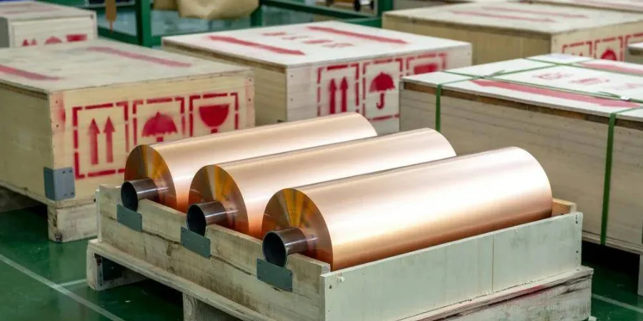
Highleap PCB Factory (HILPCB) leverages advanced copper foil technologies to manufacture high-performance circuit boards for demanding applications. Our expertise in selecting and processing various copper foil types enables optimal electrical performance, thermal management, and reliability across diverse industries from telecommunications to automotive electronics.
Copper Foil Types and Manufacturing Processes
The foundation of every PCB lies in its copper foil selection, with two primary manufacturing methods producing distinctly different characteristics suited for specific applications. Understanding these differences enables optimal material selection for each unique design requirement.
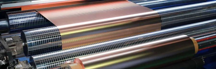
Electrodeposited (ED) Copper Foil
ED copper foil dominates PCB manufacturing due to its cost-effectiveness and excellent adhesion properties. The electrodeposition process creates a columnar grain structure with controlled roughness profiles. Standard profile ED foils feature 5-10 μm Rz roughness, providing excellent adhesion for general multilayer PCB applications. Low Profile (LP) variants with 2.5-4 μm roughness enable better etching resolution for fine-line circuits, while Very Low Profile (VLP) foils at 1.5-2.5 μm roughness support HDI and microvia board requirements. Ultra-Low Profile (ULP) foils achieving 0.8-1.5 μm roughness minimize conductor losses for high-frequency PCB applications.
Rolled Annealed (RA) Copper Foil
RA copper foil provides superior electrical and mechanical properties through its uniform grain structure achieved by mechanical rolling and annealing. This process yields tensile strength of 35-45 kgf/mm² compared to 25-35 kgf/mm² for ED foils, with elongation reaching 8-12% versus 3-8% for ED types. The remarkably smooth surface roughness of 0.3-0.8 μm Rz reduces skin effect losses by 20-30% at frequencies exceeding 1 GHz. The isotropic grain structure ensures predictable etching behavior and superior flexibility, making RA foil ideal for flex PCB applications and high-frequency circuits where conductor losses must be minimized.
Advanced Treatment Technologies
Modern copper foils undergo sophisticated surface treatments enhancing performance across multiple parameters. Zinc or brass barrier layers prevent copper migration into dielectric materials, critical for long-term reliability. Chromate conversion coatings provide oxidation resistance without impacting solderability. Silane coupling agents create chemical bonds between copper and laminate resins, improving adhesion strength by 30-50%. Nodularization treatments balance adhesion requirements with signal integrity needs, allowing optimization for specific frequency ranges and applications.
High-Frequency Performance and Signal Integrity
At frequencies exceeding 1 GHz, copper foil characteristics significantly impact signal propagation and losses. The skin effect phenomenon confines current flow to increasingly shallow depths at the conductor surface, making surface roughness a critical parameter for high-frequency design.
Understanding Skin Depth Effects
The skin depth in copper decreases dramatically with frequency, measuring 66 μm at 1 MHz but only 2.1 μm at 1 GHz. At automotive radar frequencies of 77 GHz, skin depth shrinks to merely 0.24 μm. When skin depth approaches the magnitude of surface roughness, conductor losses increase exponentially. Even VLP foils with 1.5 μm roughness create significant additional loss at millimeter-wave frequencies, necessitating careful material selection for these applications.
Insertion Loss Components and Optimization
Total insertion loss in transmission lines comprises both dielectric and conductor components. Dielectric loss follows the relationship αd = 2.3 × f × √εr × tan δ (dB/inch), where frequency, relative permittivity, and loss tangent determine the magnitude. Conductor loss incorporates surface roughness through the correction factor Kr = 1 + (2/π) × arctan(1.4 × (Rq/δ)²), where Rq represents RMS roughness and δ denotes skin depth.
For a typical 50Ω microstrip at 10 GHz, smooth foil with 0.3 μm Rq roughness exhibits conductor loss around 0.15 dB/inch, while standard foil with 2.5 μm Rq roughness increases losses to approximately 0.35 dB/inch. This 133% increase in conductor loss significantly impacts link budgets for high-frequency systems.
Phase Stability and Roughness Effects
Surface roughness creates phase variations critical for phased array antennas and precision timing circuits. The effective dielectric constant increases due to roughness according to εeff_rough = εeff_smooth × (1 + ΔRq/h), where h represents dielectric thickness and ΔRq the RMS roughness differential. This effect causes frequency-dependent phase shifts that complicate wideband designs and degrade beam steering accuracy in antenna arrays.
Heavy Copper Technology for Power Applications
Heavy copper PCB technology utilizing copper weights from 3 oz/ft² (105 μm) to 20 oz/ft² (700 μm) enables unprecedented current carrying capacity and thermal management capabilities essential for modern power electronics.
Current Capacity Enhancement
The IPC-2152 standard provides comprehensive guidelines for conductor sizing based on acceptable temperature rise. A 0.25mm wide trace in standard 1 oz copper carries approximately 1.9A externally with 20°C temperature rise. The same width in 4 oz copper handles 5.1A, while 10 oz copper manages 9.8A under identical conditions. Internal layers exhibit roughly 50% current capacity due to reduced convection cooling. These dramatic improvements enable compact power distribution networks handling kilowatts within reasonable board areas.
Thermal Management Through Copper Mass
Heavy copper's exceptional thermal conductivity of 385 W/m·K enables efficient heat spreading from localized sources. Thermal resistance reduces by 70-85% compared to standard copper weights, typically decreasing junction temperatures by 15-25°C. This improvement often eliminates requirements for external heatsinks, reducing system cost and complexity while improving reliability through lower operating temperatures.
Specialized Manufacturing Processes
Processing heavy copper demands adapted techniques throughout the manufacturing flow. Blue-tack lamination prevents resin starvation between thick copper features, maintaining dielectric integrity. Extended etching cycles with continuous chemistry regeneration ensure uniform feature definition despite increased copper thickness. Drilling parameters require reduced feed rates and specialized bit geometries preventing excessive heat generation. Plating chemistry modifications accommodate higher aspect ratios and ensure uniform thickness distribution across varying feature densities.
Surface Treatments and Copper Foil Protection
Protecting copper surfaces from oxidation while maintaining solderability and assembly compatibility requires carefully selected finishes matched to specific application requirements and assembly processes.
ENIG (Electroless Nickel Immersion Gold)
ENIG provides excellent protection through 3-6 μm nickel barrier layers topped with 0.05-0.2 μm gold. This combination offers exceptional shelf life exceeding 12 months while maintaining wire bondability for semiconductor packaging applications. The nickel barrier prevents copper diffusion, critical for long-term reliability in harsh environments. However, the nickel layer's magnetic properties and relatively high resistance can impact high-frequency performance.
Immersion Silver and OSP Alternatives
Immersion silver deposits 0.12-0.40 μm of pure silver, providing lower insertion loss than ENIG for RF applications due to silver's superior conductivity. Limited shelf life of 6-12 months requires careful storage and handling to prevent tarnishing. OSP (Organic Solderability Preservative) coatings apply ultra-thin 0.2-0.5 μm organic films with minimal impact on high-frequency performance. Modern OSP formulations support multiple reflow cycles, making them cost-effective for large-volume assembly applications.
Application-Specific Selection Criteria
Surface finish selection depends on multiple factors including assembly process, operating environment, shelf life requirements, and electrical performance needs. High-frequency applications favor immersion silver or OSP for minimal conductor impact. Wire bonding applications require ENIG or ENEPIG finishes. Lead-free assembly processes may exclude certain finishes due to temperature limitations or wetting characteristics.
Advanced Copper Foil Solutions for Hybrid PCBs
Hybrid PCBs introduce complex material interactions that demand more than just standard copper foil choices. At HILPCB, we provide copper foil strategies tailored to each substrate—whether it's PTFE, ceramic, FR-4, or polyimide—to ensure optimal adhesion, thermal balance, and high-frequency performance.
Our team supports your design from the start, offering stackup consulting, foil type selection, and thermal stress management strategies to prevent warpage, delamination, or signal degradation across mixed-material layers.
From concept to production, we help you unlock the full potential of hybrid PCBs—balancing performance, reliability, and cost through expert copper integration and manufacturing precision.
Frequently Asked Questions
What copper weight should I use for high-current applications?
Copper weight selection depends on current requirements, available space, and thermal constraints. For currents exceeding 10A, consider 3-4 oz copper minimum. Use IPC-2152 calculators accounting for ambient temperature, acceptable temperature rise, and adjacent heating sources. Heavy copper PCB technology up to 20 oz enables extreme current handling when space permits.
How does copper roughness affect high-frequency performance?
Surface roughness significantly impacts conductor losses above 1 GHz through increased effective resistance. Rough surfaces increase path length and create field concentrations. For frequencies exceeding 10 GHz, specify VLP or ULP foils with Rz below 2 μm. At 77 GHz automotive radar frequencies, even minimal roughness can double conductor losses compared to ideally smooth surfaces.
What's the difference between ED and RA copper foils?
ED (electrodeposited) foils offer superior adhesion through controlled roughness profiles and lower cost for general applications. RA (rolled annealed) foils provide better flexibility with 50% higher elongation, lower conductor losses through smoother surfaces, and superior mechanical properties. Choose ED for standard rigid boards and RA for flex circuits or demanding high-frequency designs above 10 GHz.
Can different copper weights be used in the same PCB?
Yes, selective copper plating enables varying thicknesses within single layers. Starting with base copper (typically 0.5 oz), specific areas plate up to required thickness. This technique optimizes current capacity in power sections while maintaining fine features for signals. Consider thermal balance across the board to prevent warpage during assembly.
How do I specify copper foil for impedance-controlled designs?
Specify both copper weight and roughness profile for accurate impedance control. For ±5% impedance tolerance, maintain consistent foil types throughout the stackup. Our impedance calculator accounts for roughness effects on effective dielectric constant. Provide target impedance, tolerance requirements, and operating frequency range for optimal foil selection recommendations.
What copper treatments prevent oxidation during storage?
All exposed copper surfaces require protection from oxidation. OSP provides 6-month shelf life with minimal thickness impact. Immersion silver extends protection to 12 months with excellent solderability. ENIG offers 12+ months shelf life with wire bonding capability. For extended storage, specify moisture barrier packaging with desiccants and humidity indicators maintaining below 30% RH.