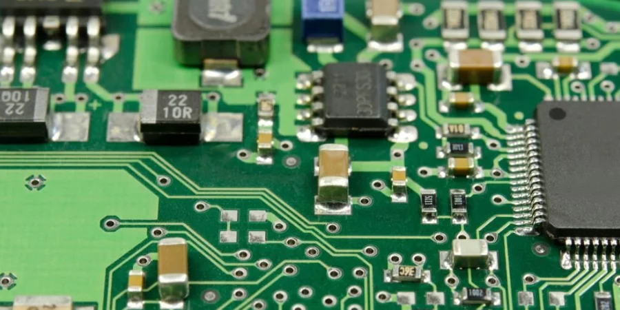
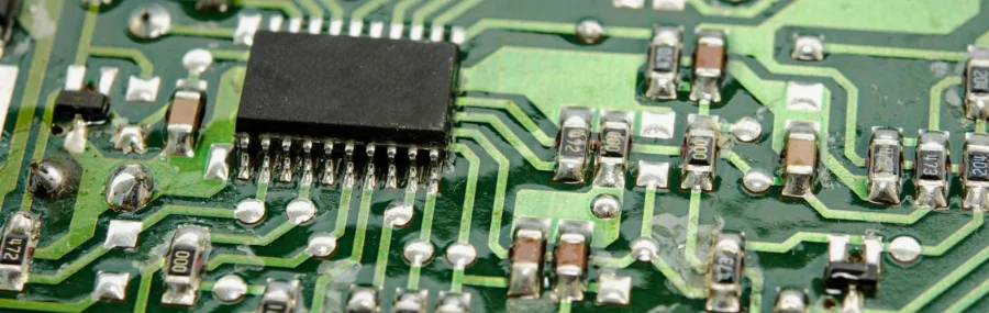
At HILPCB, we offer comprehensive PCB manufacturing capabilities, producing all types of PCBs to meet diverse project requirements. Among our specialties is high-frequency PCB production, ensuring optimal signal integrity and performance in applications such as telecommunications and high-speed digital systems.
Our expertise in insulation materials and testing guarantees that your designs meet strict safety standards while maintaining electrical performance, whether for consumer electronics, industrial applications, or high-voltage power systems. With ISO 9001-certified processes, we deliver consistent quality and reliability across all PCB types.
Understanding PCB Insulation Properties and Requirements
PCB insulation forms the foundation of electrical safety and performance in modern electronics. The dielectric material between conductive layers must provide adequate electrical isolation while supporting mechanical structure and thermal management. Understanding key insulation parameters enables optimal material selection for specific applications.
Dielectric strength represents the maximum electric field a material withstands before breakdown occurs. Standard FR-4 PCB materials exhibit dielectric strength of 20-28 kV/mm, sufficient for most applications. However, high-voltage designs require enhanced materials achieving 40-60 kV/mm. The relationship between applied voltage and insulation thickness follows V = E × d, where breakdown voltage equals dielectric strength multiplied by material thickness.
Surface and volume resistivity characterize insulation resistance under different conditions. Surface resistivity, measured in ohms per square, indicates contamination susceptibility and leakage current potential. Volume resistivity, expressed in ohm-centimeters, determines bulk current flow through the dielectric. Quality PCB insulation maintains surface resistivity above 10^12 Ω/□ and volume resistivity exceeding 10^14 Ω·cm under standard conditions.
Comparative Tracking Index (CTI) quantifies insulation performance under contamination and moisture exposure. Materials rated CTI 600+ suit harsh environments, while CTI 175-400 suffices for controlled conditions. This parameter proves critical for automotive and outdoor applications where environmental factors compromise insulation integrity.
Advanced PCB Insulation Materials Selection
Modern PCB manufacturing employs diverse insulation materials optimized for specific electrical, thermal, and mechanical requirements. Each material category offers distinct advantages addressing unique application challenges.
Glass-Epoxy Systems (FR-4 and Variants)
Standard FR-4 remains the workhorse of PCB insulation, balancing cost, performance, and manufacturability. Enhanced variants like high-Tg PCB materials extend temperature capability from 130°C to 170-200°C, crucial for lead-free assembly and high-temperature operation. The glass transition temperature directly impacts dimensional stability and insulation reliability at elevated temperatures.
Polyimide Flexible Substrates
Polyimide films provide exceptional insulation for flex PCB applications, maintaining properties from -269°C to +400°C. The material's 3.5 dielectric constant and 0.002 dissipation factor enable high-frequency performance while providing mechanical flexibility. Adhesiveless constructions eliminate weak interfaces, improving insulation reliability in dynamic applications.
PTFE and Ceramic-Filled Composites
High-frequency designs leverage PTFE-based materials achieving dielectric constants from 2.1 to 10.2 through ceramic loading. These materials maintain stable insulation properties across frequency and temperature ranges, essential for high-frequency PCB applications. The low dissipation factor (0.0009-0.002) minimizes signal loss while providing excellent electrical isolation.
Specialized High-Voltage Insulation
Power electronics demand enhanced insulation systems surviving partial discharge and corona effects. Specialized resins with ceramic fillers achieve breakdown voltages exceeding 100 kV/mm in thin films. Multi-layer insulation strategies combining different materials optimize performance - for example, using polyimide films between FR-4 layers doubles breakdown voltage while maintaining processability.
Design Strategies for Optimal PCB Insulation
Effective PCB insulation design extends beyond material selection to encompass layout techniques maximizing electrical isolation and reliability. Strategic implementation of design rules prevents field failures while optimizing manufacturing yield.
Creepage and Clearance Calculations
IPC-2221 provides baseline spacing requirements based on voltage and environmental conditions. For voltages exceeding 500V, creepage distances must account for pollution degree and CTI ratings. Calculate minimum creepage using: L = V × k, where k ranges from 0.6 to 2.5 mm/kV depending on conditions. Clearance requirements consider altitude effects, with spacing increasing 3% per 1000m elevation above 2000m.
Slot and Barrier Implementation
Physical slots between high-voltage sections extend creepage paths without increasing board size. Routed slots 0.5-2.0mm wide force surface currents to travel around openings, effectively doubling creepage distance. Conformal coating barriers create similar effects using selective application of high-CTI materials along critical boundaries.
Guard Ring and Shield Techniques
Guard rings surrounding sensitive circuits intercept leakage currents before reaching protected areas. Connected to appropriate bias voltages, these structures maintain consistent electric fields preventing insulation degradation. Electrostatic shields between layers block capacitive coupling while preserving DC isolation - critical for mixed-signal designs combining power and precision analog circuits.
Testing and Validation of PCB Insulation Systems
Comprehensive testing validates PCB insulation performance under worst-case conditions, ensuring long-term reliability. HILPCB implements rigorous test protocols exceeding industry standards.
Hipot and Insulation Resistance Testing
Dielectric withstanding voltage (DWV) testing applies specified voltages between isolated nets, detecting marginal insulation. Test voltages typically equal 2×Vworking + 1000V for one minute. Insulation resistance measurements at 500-1000VDC quantify leakage current, with acceptance criteria requiring >10^9 Ω minimum. Temperature and humidity preconditioning reveals moisture sensitivity effects.
Partial Discharge Analysis
High-voltage applications require partial discharge testing identifying localized breakdown precursors. Corona inception voltage indicates long-term reliability margins. Advanced phase-resolved partial discharge patterns distinguish defect types - voids show symmetric patterns while delamination creates asymmetric signatures. This analysis prevents field failures in power electronics applications.
Environmental Stress Validation
Accelerated aging combines temperature, humidity, and voltage stress revealing insulation degradation mechanisms. Temperature cycling (-40°C to +125°C) induces mechanical stress at material interfaces. Highly Accelerated Stress Testing (HAST) at 130°C/85%RH accelerates moisture ingress effects. Thermal shock testing validates insulation integrity across extreme temperature transitions encountered in automotive and aerospace applications.
Manufacturing Excellence for Reliable PCB Insulation
HILPCB's manufacturing processes ensure consistent insulation properties through precise control and comprehensive quality systems. Our approach addresses critical factors affecting insulation reliability.
Lamination Process Control
Proper resin flow during multilayer PCB lamination eliminates voids compromising insulation. Optimized pressure profiles ensure complete wet-out while preventing excessive resin depletion. Vacuum-assisted lamination removes entrapped air, achieving void-free insulation layers. Post-lamination bake cycles complete cross-linking reactions maximizing insulation properties.
Contamination Prevention
Ionic contamination degrades insulation resistance, particularly under humidity exposure. Our processes maintain cleanliness below 1.56 μg/cm² NaCl equivalent through optimized cleaning chemistry and deionized water rinses. Automated ionic contamination testing validates every production lot. Clean room environments for critical processes prevent particulate contamination creating breakdown paths.
Surface Treatment Optimization
Controlled surface roughness balances adhesion with insulation integrity. Excessive roughness creates stress concentrations reducing breakdown voltage, while insufficient texture compromises lamination reliability. Plasma treatment enhances wetting without damaging insulation properties. Chemical surface modification improves moisture resistance critical for long-term insulation stability.
Our turnkey assembly services include comprehensive insulation testing ensuring every delivered product meets specified safety and performance requirements.
FAQ
What PCB insulation thickness do I need for my voltage requirements?
Insulation thickness depends on working voltage and safety factors. For standard applications, use 0.1mm per 1000V working voltage as a baseline. High-reliability designs require 2-3x safety margins. Consider environmental factors - moisture exposure or altitude may necessitate additional thickness. Our engineering team provides specific recommendations based on your application requirements.
How does frequency affect PCB insulation performance?
Higher frequencies increase dielectric losses and reduce effective insulation resistance. Standard FR-4 works well below 1 GHz, while specialized materials suit higher frequencies. Dissipation factor indicates frequency-dependent losses - lower values preserve insulation integrity. For RF applications above 10 GHz, consider PTFE-based materials maintaining stable properties across frequency ranges.
What causes PCB insulation failure over time?
Common failure mechanisms include moisture absorption, ionic contamination, thermal degradation, and mechanical stress. Moisture reduces insulation resistance exponentially - 1% absorption can decrease resistance 100x. Thermal cycling creates mechanical stress at material interfaces. Proper material selection and protective coatings mitigate these effects, extending insulation life beyond 20 years.
Can I improve existing PCB insulation without redesigning?
Yes, several methods enhance insulation post-fabrication. Conformal coatings add 500-1500V breakdown strength per 25μm thickness. Parylene coating provides exceptional moisture barriers. Underfill materials eliminate air gaps in high-voltage assemblies. However, design-stage optimization proves more effective than post-process treatments.
How do I specify PCB insulation requirements effectively?
Clearly define working voltage, environmental conditions, and lifetime requirements. Specify applicable standards (IPC-2221, IEC 60950, UL 796). Include CTI requirements for harsh environments. Define test methods and acceptance criteria. Our Gerber viewer helps verify spacing rules during design review.
What's the difference between functional and safety insulation?
Functional insulation separates circuits for proper operation without safety implications. Safety insulation protects users from hazardous voltages, requiring higher reliability and specific regulatory compliance. Safety insulation demands reinforced or double insulation systems, comprehensive testing, and ongoing quality monitoring per safety standards like IEC 61010.