Highleap PCB Factory (HILPCB) delivers comprehensive PCB manufacturing and assembly solutions with advanced solderability testing capabilities. Our expertise encompasses wetting balance analysis, surface finish evaluation, and component lead testing, ensuring optimal solder joint formation that prevents assembly defects, cold joints, and reliability issues before final product integration across diverse electronic applications.
Core PCB Solderability Testing Methods and Technologies
PCB solderability testing is a critical quality control process in electronics manufacturing. It verifies surface wettability, detects oxidation or contamination, and ensures compatibility with assembly processes. Using standardized methodologies and quantitative techniques, solderability testing provides objective validation of both PCB finishes and component terminations.
Advanced Solderability Testing Techniques:
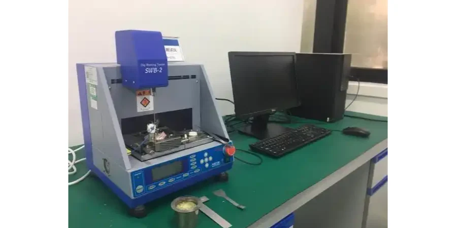
- Wetting Balance Test: Offers high-resolution (±0.01 mN) force measurement to quantitatively evaluate solder wetting dynamics over time.
- Dip-and-Look Method: A widely adopted visual technique per IPC J-STD-002/003, used for rapid assessment of wetting acceptability.
- Steam Aging Simulation: Exposes samples to 93 ± 3°C for defined durations (typically 8 hours) to simulate long-term storage effects on solderability.
- Surface Analytical Tools: Techniques such as X-ray Photoelectron Spectroscopy (XPS) and SEM-EDS are used to identify surface oxidation levels and organic contamination.
- Component Lead Evaluation: Critical for fine-pitch and BGA packages; tests individual lead terminations for solder wetting performance.
- Solder Spread Test: Measures the spread area of molten solder to quantify substrate wettability.
- Contact Angle Measurement: Directly measures the angle between molten solder and pad surface to evaluate interfacial behavior.
- Globule Test: Assesses solder ball formation and coalescence on specific surface finishes, such as OSP or ENIG.
- Thermal Profiling: Ensures test conditions align with actual assembly reflow or wave soldering temperatures for realistic validation.
Effective solderability control involves selecting appropriate test methods based on surface finish type, component geometry, and end-use environment. At HILPCB, we leverage a combination of these techniques within a tightly controlled manufacturing workflow. This allows us to maintain consistent solder joint quality across diverse board types, from FR4 PCBs to advanced metal core PCBs, optimizing both reliability and production efficiency.
Surface Finish Evaluation and Aging Characteristics
Different PCB surface finishes exhibit unique solderability profiles that evolve through storage and environmental exposure, requiring finish-specific testing approaches to ensure reliable assembly performance.
HASL and Lead-Free HASL Performance: Hot Air Solder Leveling provides inherent solderability through pre-tinned surfaces but faces thickness variation challenges. Testing must account for uneven topography affecting fine-pitch assembly. Lead-free HASL variants require higher test temperatures (245-255°C) compared to traditional tin-lead systems. Accelerated aging reveals minimal degradation over 12-month equivalent storage when properly packaged.
OSP Coating Degradation Analysis: Organic Solderability Preservatives offer excellent flatness for high-density interconnect HDI PCB applications but demonstrate limited thermal stability. Multiple reflow cycles progressively degrade the organic layer, requiring careful testing after each thermal exposure. Standard OSP coatings maintain acceptable solderability through 2-3 reflow cycles, while high-temperature variants extend this to 5-6 cycles. Testing protocols must simulate actual assembly thermal profiles.
ENIG Black Pad Detection: Electroless Nickel Immersion Gold finishes require specialized testing to detect potential black pad defects. Standard wetting tests may show acceptable results while masking underlying nickel corrosion. Cross-sectional analysis combined with extended dwell time testing reveals problematic interfaces. Gold thickness measurement ensures optimal 0.05-0.08μm range preventing excessive gold embrittlement while maintaining shelf life.
Wetting Balance Analysis and Quantitative Measurement
The wetting balance test provides objective, repeatable measurement of soldering dynamics through continuous force monitoring during controlled solder immersion, generating data-rich wetting curves for detailed analysis.
Force-Time Curve Interpretation:
• Initial Buoyancy Phase: Negative force proportional to sample volume and solder density • Wetting Transition: Force reversal indicating meniscus formation and wetting initiation • Maximum Force Achievement: Plateau representing equilibrium between wetting and gravity forces • Key Parameters: T0 (zero crossing time) <1s and F(max) >2mN/mm perimeter for acceptable wetting • Curve Shape Analysis: Smooth transitions indicate uniform wetting; irregularities suggest contamination • Temperature Effects: 10°C increase typically reduces T0 by 15-20% due to improved flux activity • Flux Comparison: Wetting curves differentiate flux effectiveness for specific surface finishes • Statistical Validation: Minimum 5 samples per test condition ensuring 95% confidence intervals • SMT assembly Correlation: Direct relationship between wetting parameters and assembly first-pass yields
Integration of Solderability Control in PCB Manufacturing and Assembly
In-Line Solderability Control During PCB Fabrication
Effective solderability assurance begins at the fabrication stage. At HILPCB, we implement process checkpoints throughout the PCB production line to verify solderable surface integrity:
- Post-solder mask inspection: After solder mask application, test coupons are evaluated to ensure exposed pads remain free of contamination and oxidation.
- Surface finish validation: For finishes such as HASL, ENIG, and ImmAg, solderability is verified immediately after plating using wetting tests and surface thickness measurements.
- Multilayer PCB via reliability: In high-layer count boards, via filling and plating steps undergo targeted testing to ensure interconnects support robust solder joints during later assembly.
This real-time monitoring reduces downstream failure risks and ensures consistency across high-complexity boards like multilayer PCBs.
Solderability Assurance in PCBA Assembly Lines
Solderability directly influences SMT yield and solder joint reliability. Our PCBA process integrates pre-assembly checks and inline control to mitigate risks:
- Board flatness and pad condition: Warpage measurement and solderability tests are performed before stencil printing to avoid bridging or insufficient contact.
- Component lead integrity: Incoming inspection includes solderability testing for passive and active component leads, including BGA spheres, to prevent non-wetting and cold joints.
- Correlation with actual solder joints: Data from inline SPI and AOI systems are cross-referenced with pre-assembly solderability results, allowing predictive process adjustments.
- First article inspection (FAI): Each production run undergoes FAI including cross-section analysis of solder joints, validating the test data against real-world reflow performance.
This methodology strengthens outcomes in both small-batch assemblies and high-volume production.
Batch-Level Control and Full Traceability
Maintaining traceability of solderability test results is critical for quality assurance and root cause analysis. HILPCB applies strict batch management practices:
- Lot-based test segregation: Boards that show borderline solderability are flagged for alternate reflow profiles or flux enhancement to improve yield.
- Date-code tracking: Ensures FIFO (first-in, first-out) usage to prevent solderability degradation due to prolonged storage.
- Barcode integration: Every PCB is labeled with a unique code linking it to solderability test records, assembly parameters, and process history.
This traceability is essential for industries requiring full process transparency, such as aerospace, medical devices, and automotive electronics. It also enables efficient failure analysis and corrective actions in turnkey PCB assemblies.
Troubleshooting Common Solderability Issues
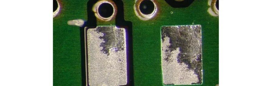
Solderability failures such as non-wetting are often caused by oxidation or surface contamination. These issues prevent solder from adhering properly to component leads or PCB pads. At HILPCB, we utilize analytical methods such as SEM imaging and contact angle measurement to pinpoint the root causes. Plasma cleaning is used to eliminate organic contaminants, while chemical reduction treatments restore oxidized copper or tin surfaces. Affected production lots are isolated for traceability and corrective action while maintaining quality flow in SMT assembly and through-hole processes.
De-wetting occurs when solder initially wets but later recedes, leaving exposed areas. This typically results from incompatible flux chemistries, thermal overstress, or contamination in solder baths. Excessive intermetallic compound growth, especially in high-temperature reflow profiles, also contributes to this issue. Our process team mitigates de-wetting by optimizing reflow curves, verifying flux activation levels, and regularly analyzing solder pot composition. These controls are critical for assemblies using high-Tg PCBs and performance-sensitive high-frequency PCBs.
When wetting inconsistencies are localized rather than widespread, common causes include surface finish variation, stencil misalignment, or pad contamination from improper handling. In such cases, we perform targeted microscopic inspection and cross-sectional analysis. Process corrections may involve localized cleaning, review of rinsing procedures, or stencil alignment verification. For complex builds like rigid-flex PCBs or ceramic PCBs, even minor inconsistencies can significantly impact reliability, requiring tighter controls and frequent first-article validation.
HILPCB's Integrated Approach to Solderability Excellence
As a leading China PCB manufacturer, HILPCB integrates solderability considerations throughout the production process rather than treating it as an isolated test. Our approach begins with material selection, continues through process optimization, and culminates in comprehensive testing ensuring every PCB meets stringent solderability requirements.
Design-Integrated Solderability: Our engineering team reviews designs for solderability risk factors including pad geometries, mask definitions, and finish specifications. Early identification of potential issues enables design optimization preventing downstream assembly challenges. We maintain extensive databases correlating design features with solderability performance.
Process Control Excellence: Real-time monitoring of critical parameters—bath chemistry, temperatures, and dwell times—ensures consistent surface finish quality. Statistical process control identifies trends before they impact solderability. Our ISO 9001 certified processes incorporate solderability checkpoints at multiple stages, not just final inspection.
Comprehensive Testing Capabilities: Our laboratory features multiple wetting balance systems, steam aging chambers, and surface analysis equipment. This infrastructure supports both routine quality control and advanced failure analysis. We provide detailed test reports including wetting curves, statistical analysis, and photographic documentation supporting customer quality requirements.
PCB Solderability Testing – FAQ
What constitutes acceptable PCB solderability test results? Acceptable results show uniform solder coverage exceeding 95% of the test area, contact angles below 30 degrees, and wetting times under 1 second at specified temperatures. Quantitative criteria vary by application and standard.
How does storage time affect PCB solderability? Solderability degrades predictably over time following oxidation kinetics. Properly stored boards maintain acceptable solderability for 12 months (HASL), 6 months (OSP), or 24 months (ENIG). Nitrogen storage extends these periods significantly.
Which solderability test method provides the most reliable results? Wetting balance testing offers superior quantitative data and repeatability. However, test method selection depends on application requirements, with visual methods suitable for screening and wetting balance for detailed characterization.
Can solderability be restored after failure? Limited restoration is possible through plasma cleaning or chemical reduction, but results vary by failure mechanism. Prevention through proper storage and handling proves more effective than restoration attempts.
What environmental factors most impact solderability? Temperature, humidity, and atmospheric contamination significantly affect solderability. High humidity accelerates oxidation while sulfur-containing atmospheres tarnish silver finishes. Controlled storage environments minimize degradation.
How do lead-free requirements change solderability testing? Lead-free assembly requires higher test temperatures (245-260°C), different flux chemistries, and modified acceptance criteria. Test methods remain similar but parameters adjust for lead-free solder characteristics.