At Highleap PCB Factory (HILPCB), we support a wide range of advanced PCB manufacturing requirements—including peelable solder mask options for complex assembly scenarios. This removable mask helps protect gold fingers, plated-through holes, or other critical areas during wave soldering, selective soldering, or conformal coating, eliminating the need for manual taping or secondary processing.
As part of our full-service PCB production capabilities, peelable mask solutions are available on request to simplify your assembly workflow while ensuring clean, residue-free removal after processing.
Critical Applications for Peelable Mask PCB Technology
Peelable mask serves essential functions in modern PCB assembly where permanent solder mask cannot provide adequate protection. During mixed-technology assembly combining SMT assembly and through-hole assembly, previously soldered SMT components require protection from wave solder exposure. The temporary mask prevents solder bridging, component damage, and contamination of sensitive areas.
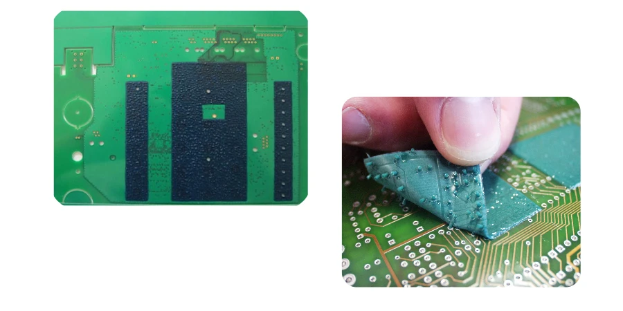
Gold finger protection during assembly represents another critical application. Contact fingers requiring post-assembly gold plating must remain solder-free, yet permanent solder mask would prevent plating access. Peelable mask provides temporary protection during soldering, then removes cleanly for subsequent plating operations. This approach eliminates expensive selective plating fixtures while ensuring consistent quality.
Conformal coating masking proves particularly valuable for aerospace and automotive applications. Connectors, test points, and adjustment potentiometers must remain coating-free for functionality. Traditional masking tapes require manual application and removal, adding labor cost and quality variation. Screen-printed peelable mask ensures precise, repeatable coverage while reducing assembly time by 60-80% compared to manual methods.
Material Selection and Process Compatibility
Modern peelable mask materials offer distinct advantages for different applications:
Latex-Based Formulations
- Temperature resistance: Up to 180°C
- Removal window: 7-14 days optimal
- Cost: Most economical option
- Limitations: Allergen concerns, limited reflow compatibility
Water-Based Acrylic Systems
- Temperature resistance: 260°C lead-free compatible
- Curing temperature: 80-120°C
- Environmental compliance: Zero VOC
- Removal characteristics: Clean peel up to 60 days
Synthetic Rubber Compounds
- Temperature resistance: 280°C+ for specialized applications
- Chemical resistance: Superior for harsh processes
- Flexibility: Maintains properties at -40°C to +150°C
- Application: Ideal for thick deposits and 3D coverage
Critical Process Parameters:
Thickness specifications vary by application:
- Flat surface protection: 0.1-0.2mm
- Component coverage: 0.3-0.5mm
- Wave solder fixtures: 0.5-1.0mm
- Conformal coat masking: 0.15-0.25mm
Screen printing parameters:
- Mesh count: 60-80 threads/inch for standard applications
- Emulsion thickness: 20-50μm over mesh
- Snap-off distance: 3-5mm
- Print speed: 50-100mm/second
- Squeegee angle: 45-60 degrees
The removal window represents a critical but often overlooked specification. Environmental factors significantly impact adhesion over time - UV exposure can reduce the removal window by 50%, while humidity accelerates adhesion in some formulations. Establishing documented removal schedules based on your specific storage conditions ensures consistent, damage-free removal.
Design Guidelines for Peelable Mask Implementation
Effective peelable mask implementation requires careful design consideration from the initial PCB layout stage:
Critical Design Rules:
→ Mask Boundary Extensions
- Minimum 0.5mm beyond protected area for registration tolerance
- 1.0mm preferred for wave solder applications
- 2.0mm for areas requiring complete seal
→ Corner Radius Requirements
- Internal corners: 0.5mm minimum radius
- External corners: 0.3mm minimum radius
- Prevents tearing during removal
- Improves material flow during application
→ Component Clearances
- QFP/QFN packages: 0.3mm minimum from pad edge
- BGA arrays: 0.5mm from outermost balls
- 0402 components: 0.2mm clearance
- Connectors: Follow manufacturer keep-out zones
Documentation Best Practices:
The success of peelable mask application heavily depends on clear communication between design and manufacturing teams. Your fabrication data package should include:
Dedicated Gerber Layer
- Use unique layer naming (e.g., .GPM for top peelable mask)
- Different color coding from permanent mask
- Clear notes on layer function
Assembly Drawings
- Removal timing specifications
- Temperature exposure limits
- Areas requiring special attention
- Reference photos of correct application
3D Models
- Include mask thickness in step files
- Highlight areas of concern
- Verify fixture compatibility
Poor documentation causes 30% of peelable mask failures. Investment in comprehensive documentation pays dividends through reduced scrap and faster production ramp-up.
Manufacturing Process Integration and Quality Control
Integration of peelable mask into standard multilayer PCB manufacturing requires process validation ensuring compatibility with existing operations. Screen printing parameters including squeegee pressure, speed, and snap-off distance require optimization for each mask material. Typical print speeds range from 50-100mm/second with 3-5mm snap-off distance.
Curing profiles must balance complete polymerization against substrate thermal limits. Conveyor ovens set at 100-120°C with 5-10 minute dwell times suit most acrylic formulations. Insufficient curing causes poor adhesion and process survival, while excessive temperature may damage temperature-sensitive components or substrates.
Quality inspection focuses on coverage completeness, thickness uniformity, and adhesion level. Visual inspection under 10X magnification reveals pinholes, thin areas, or contamination. Adhesion testing using calibrated peel tests ensures sufficient bonding without excessive force requirements for removal. Statistical process control tracks these parameters, identifying trends before defects occur.
Cost-Benefit Analysis and ROI Considerations
Implementing peelable mask technology requires initial investment in screen preparation and process development, typically $500-2000 per design. However, labor savings quickly offset these costs. Manual masking operations average 2-5 minutes per board depending on complexity. Peelable mask application adds only seconds to screen printing operations, reducing labor cost by 80-90%.
Material costs range from $0.10-0.50 per board depending on coverage area and thickness. Compare this to manual masking tape costs of $0.05-0.15 plus significantly higher labor expenses. For production volumes exceeding 100 pieces, peelable mask provides clear economic advantages while improving consistency and reliability.
Quality improvements further enhance ROI. Manual masking variations cause 2-5% defect rates from incomplete coverage or residue contamination. Properly implemented peelable mask reduces defects below 0.5%, eliminating rework costs and delivery delays. For high-reliability applications, these quality improvements justify implementation regardless of volume considerations.
FAQ
When should I consider peelable mask versus permanent solder mask?
Use peelable mask when areas require temporary protection during specific processes but need exposure afterward. Common scenarios include gold finger protection during wave soldering, keep-out areas for conformal coating, and protecting installed components during selective soldering. Permanent mask suits areas requiring lifetime protection.
What's the typical turnaround time impact of adding peelable mask?
Adding peelable mask to existing designs typically extends production by 1-2 days for screen preparation and process setup. Subsequent orders require no additional time as the screen printing operation integrates into standard assembly flow. For turnkey assembly projects, we parallelize these operations minimizing impact.
Can peelable mask survive multiple reflow cycles?
Quality peelable masks withstand 2-3 standard lead-free reflow cycles (260°C peak) without degradation. However, each thermal cycle slightly increases adhesion, potentially complicating removal. For applications requiring multiple high-temperature exposures, specify high-temperature formulations and plan removal immediately after final thermal process.
How does peelable mask affect PCB testability?
Peelable mask can cover test points during assembly, then remove for in-circuit testing. This protects test pads from solder contamination while maintaining full test access. Design test fixtures accounting for mask thickness variations. Some manufacturers leave mask in place, testing through the material using spring-loaded probes.
What are the environmental considerations?
Modern water-based peelable masks contain no hazardous air pollutants (HAPs) or ozone-depleting substances. Removed mask material qualifies as non-hazardous solid waste in most jurisdictions. UV-curable formulations further reduce environmental impact by eliminating solvents and reducing energy consumption during curing.
Can peelable mask be reworked if application errors occur?
Fresh uncured mask removes easily with appropriate solvents, typically water for acrylic types or alcohol for rubber-based materials. Once cured, removal becomes difficult without damaging the PCB surface. Prevention through proper process control proves more effective than attempting rework. Design reviews catching potential issues early prevent costly errors.