Looking for a reliable partner in PTFE PCB manufacturing? We specialize in high-frequency PCB production using advanced PTFE-based materials from top suppliers like Rogers, Taconic, Arlon, and Isola. With decades of experience and precision-focused processes, we deliver low-loss, high-stability PCBs tailored for RF, microwave, and millimeter-wave applications—on time and to spec.
PTFE PCB Manufacturing Services
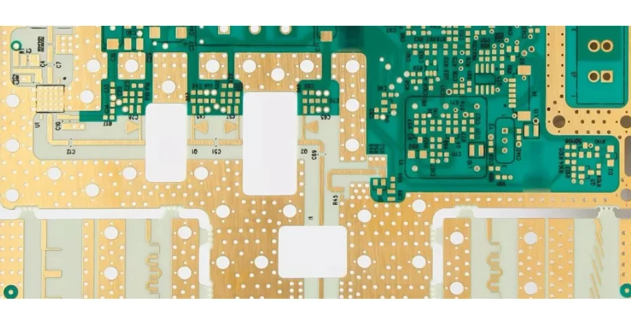
PTFE (Polytetrafluoroethylene) based laminates represent the gold standard for high-frequency PCB applications demanding ultra-low loss and stable electrical properties. We process all major PTFE material systems including pure PTFE, ceramic-filled PTFE, and glass-reinforced PTFE composites from leading suppliers like Rogers, Taconic, Arlon, and Isola. Our expertise spans Rogers RT/duroid series (5870, 5880, 6002), Taconic RF and TLY series, Arlon DiClad and CuClad series, delivering consistent results with dielectric constants ranging from 2.1 to 10.2 and dissipation factors as low as 0.0009.
The unique properties of PTFE - including its low dielectric constant, minimal moisture absorption, and exceptional chemical resistance - require specialized handling throughout the manufacturing process. Our climate-controlled facility maintains optimal temperature and humidity levels to prevent dimensional changes during processing. We employ dedicated tooling for PTFE materials to avoid cross-contamination and ensure pristine surface quality essential for reliable copper adhesion.
Specialized Manufacturing Processes for PTFE Circuit Boards
PTFE PCB fabrication demands precise control at every stage due to the material's unique characteristics. Our drilling operations utilize specialized carbide drill bits with optimized geometries to manage PTFE's tendency to smear and deform. We maintain strict control over drilling parameters including spindle speed (typically 50-70k RPM), feed rates, and pecking cycles to achieve clean hole walls essential for reliable plated through holes. Entry and exit materials are carefully selected to minimize burring and fiber protrusion.
Surface preparation for PTFE substrates employs sodium etching or plasma treatment to modify the naturally non-stick surface for enhanced copper adhesion. Our metallization process includes specialized seed layers and electroless copper formulations optimized for PTFE materials. The subsequent electrolytic plating builds copper thickness while maintaining uniform distribution critical for impedance control in microstrip and stripline configurations.
Design Considerations for PTFE PCB Success
| Design Parameter | PTFE-Specific Consideration | Our Manufacturing Capability |
|---|---|---|
| Via Structure | Larger annular rings recommended | 0.1mm minimum via, 0.05mm annular ring |
| Copper Adhesion | Requires special surface treatment | Peel strength >8 lb/in achieved |
| Dimensional Stability | CTE mismatch considerations | Pre-conditioning and stress relief |
| Impedance Control | Tighter tolerances due to Dk variations | ±5% standard, ±3% available |
| Multilayer Registration | PTFE movement during lamination | ±0.075mm layer-to-layer alignment |
| Surface Finish | Limited options vs. FR-4 | ENIG, Immersion Silver, Immersion Tin |
Applications Driving PTFE PCB Demand
Aerospace and Satellite Communications
PTFE PCBs excel in space-qualified applications where low outgassing, radiation resistance, and stable performance across extreme temperatures are mandatory. We support satellite payload manufacturers with flight-qualified PTFE boards for Ka-band and Ku-band transponders, phased array antennas, and low-noise amplifiers operating from L-band through W-band frequencies.
5G and Wireless Infrastructure
The rollout of 5G networks drives demand for low-loss PTFE PCBs in massive MIMO antennas, beamforming networks, and millimeter-wave front-end modules. Our manufacturing processes ensure phase matching within ±3 degrees for antenna arrays and maintain insertion loss specifications critical for link budget optimization in 28 GHz and 39 GHz deployments.
Automotive Radar and Medical Devices
PTFE-based PCBs enable 77 GHz automotive radar sensors with superior range resolution and minimal signal attenuation. In medical applications, PTFE's biocompatibility and low loss support MRI coils, microwave ablation devices, and wireless patient monitoring systems requiring reliable performance in challenging electromagnetic environments.
Fast-Track PTFE PCB Production and Global Logistics
Understanding the urgency of product development cycles, we maintain strategic inventory of common PTFE materials including RT/duroid 5880 (0.5mm to 3.2mm), RO3003 in standard thicknesses, and TLY-5 for rapid prototyping. Our quick-turn PTFE PCB service delivers 2-layer prototypes in 48 hours and multilayer boards within 72-96 hours for standard specifications. Volume production leverages optimized panel utilization and parallel processing to achieve 5-7 day delivery for production quantities.
Our global logistics network ensures reliable delivery through partnerships with DHL Express, FedEx Priority, and specialized freight forwarders experienced in handling high-value electronics. Real-time tracking, temperature-controlled shipping options, and comprehensive insurance coverage provide peace of mind for critical shipments. We offer flexible payment terms including PayPal for rapid transactions, wire transfers with competitive exchange rates, letters of credit for international orders, and NET 30/60 terms for established accounts.
Quality Assurance and Comprehensive Testing for PTFE PCBs
Every PTFE PCB undergoes rigorous inspection exceeding IPC-6012 Class 3 requirements. Our quality protocol includes:
- Automated Optical Inspection (AOI): 100% inspection for trace integrity, spacing violations, and surface defects
- Electrical Testing: Flying probe or fixture-based testing verifying continuity and isolation resistance
- Impedance Verification: Time Domain Reflectometry (TDR) measurements with detailed reports showing location-specific values
- Microsection Analysis: Cross-sectioning for plating thickness, hole wall quality, and registration accuracy
- Environmental Testing: Thermal cycling, humidity resistance, and outgassing analysis for space applications
- RF Performance Validation: Network analyzer measurements up to 67 GHz for S-parameter verification
We maintain full traceability from raw material certification through final testing, with comprehensive documentation packages including material certificates, test reports, and impedance plots. Our ISO 9001:2015 and AS9100D certifications demonstrate commitment to consistent quality and continuous improvement.
Your Trusted PTFE PCB Manufacturer and Assembly Partner
Beyond PTFE PCB fabrication, we offer complete turnkey solutions including component sourcing, SMT/through-hole assembly, conformal coating, and functional testing. Our assembly capabilities handle fine-pitch components, high-frequency connectors, and specialized RF shields with precision placement accuracy of ±25 microns. In-circuit testing, boundary scan, and custom functional test development ensure assembled boards meet all performance specifications.
Choose a PTFE PCB manufacturer that combines technical expertise with customer-focused service. Our experienced engineering team provides free design reviews, stackup recommendations, and ongoing support throughout your project lifecycle. Whether you need quick-turn PTFE prototypes, volume production, or full turnkey assembly, we deliver quality products on time and within budget. Contact us today for competitive pricing and discover why leading aerospace, defense, and telecommunications companies trust us as their PTFE PCB manufacturing partner.