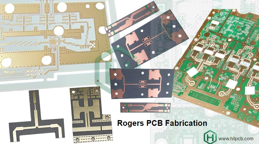
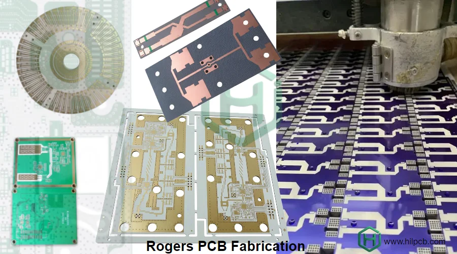
HILPCB Factory specializes in high-precision Rogers PCB fabrication and assembly, serving the RF, microwave, and 5G industries with advanced multilayer manufacturing technology. As a full-service electronics manufacturer, we provide one-stop solutions — from Rogers PCB design support and prototyping to high-volume SMT assembly and system integration — enabling global clients to bring reliable, high-performance products to market faster.
Our engineering expertise ensures optimal impedance control, dielectric stability, and thermal reliability for mission-critical applications such as radar transmitters, satellite communication modules, and next-generation wireless infrastructure.
Why Rogers Materials Dominate High-Frequency PCB Applications
In the RF and microwave domain, where frequencies exceed several gigahertz, even minute dielectric inconsistencies can degrade performance. Rogers materials outperform conventional FR-4 due to their low loss tangent, stable dielectric constant, and tight thickness tolerance, allowing precise impedance control across high-speed interconnects.
- Low Dielectric Loss (Df 0.001–0.003): Reduces insertion loss and signal distortion in long transmission lines.
- Dielectric Stability: Rogers materials maintain predictable Dk across temperature and frequency ranges, vital for phased array and mmWave antenna designs.
- Thermal and Mechanical Reliability: Low Z-axis CTE prevents via cracking during temperature cycling, while high Tg (>280 °C) ensures lead-free soldering compatibility.
- Moisture Resistance: Minimal absorption (<0.2%) keeps electrical performance consistent in outdoor or aerospace environments.
These properties make Rogers PCBs ideal for high-frequency PCB, HDI PCB, and multilayer PCB designs requiring stable performance at GHz and mmWave frequencies.
Advanced Rogers PCB Fabrication Techniques for High-Frequency Applications
At HILPCB Factory, Rogers PCB fabrication follows a precisely engineered workflow — combining material science, process control, and advanced inspection — to ensure stable impedance, low insertion loss, and repeatable high-frequency performance from prototype through mass production.
1. Material Verification and Preparation
Rogers materials require controlled storage and pre-treatment to preserve dielectric stability.
- Batch certification and Dk/Df validation: Each lot of RO4003C, RO4350B, or RT/duroid laminate is verified for dielectric and copper-clad thickness tolerance.
- Moisture and contamination control: Panels are stored under ≤40% RH and vacuum-baked before processing to eliminate moisture absorption.
- Surface activation: Plasma treatment enhances copper-to-dielectric adhesion — essential for PTFE and ceramic-filled substrates.
- Stackup confirmation: Engineering review finalizes layer order, copper weights, and reference planes for target impedance.
2. Inner Layer Imaging and Etching
Inner layers are processed using Laser Direct Imaging (LDI) for precise conductor definition:
- Achieving 25–50 μm line/space for controlled impedance transmission lines.
- AOI (Automated Optical Inspection) ensures perfect pattern alignment before lamination.
- Oxide or oxide-alternative treatment improves adhesion for multilayer bonding.
3. Lamination and Hybrid Stackup Integration
Rogers laminates often combine with FR4 PCB materials to balance cost and performance.
- PTFE-based materials use low-pressure, slow-heating lamination to prevent resin flow.
- Ceramic-filled materials (RO6002, RO4835) require precise pressure uniformity to avoid micro-fractures.
- Thermoset TMM laminates support standard multilayer lamination, offering mechanical rigidity and low CTE.
Sequential lamination supports hybrid RF/digital constructions found in 5G base stations, radar, and satellite payloads.
4. Drilling, Desmear, and Via Metallization
Drilling precision directly impacts impedance and reliability:
- Laser drilling forms blind or buried microvias (≥75 μm diameter) for compact HDI PCB structures.
- Mechanical drilling with diamond-coated bits prevents delamination in ceramic or TMM materials.
- Plasma desmear ensures clean via walls without dielectric erosion.
- Pulse plating achieves uniform copper fill in high aspect ratio vias (up to 10:1).
Via consistency and copper integrity ensure long-term reliability for mmWave circuits.
5. Outer Layer Patterning and Finishing
Outer copper layers are imaged and etched using the same LDI precision to maintain impedance control.
- Back-drilling removes unused via stubs, minimizing reflections in high-speed or differential pairs.
- Surface finishes such as ENIG, immersion silver, or hard gold are applied per assembly needs.
- Solder mask definition avoids RF areas and antenna apertures, preserving dielectric uniformity.
6. Impedance Control, Testing, and Validation
Every batch undergoes impedance modeling and verification before shipment:
- 3D field solver modeling calibrated to measured Dk/Df data.
- Inline process monitoring of copper thickness, etch depth, and dielectric spacing.
- Time Domain Reflectometry (TDR) coupons validate ±5% impedance tolerance.
- Cross-section and microsection inspection confirm trace width and via quality.
This closed-loop system ensures repeatable electrical performance across all Rogers PCB builds. HILPCB Factory’s Rogers PCB fabrication combines verified materials, precision lamination, and tight impedance validation to meet the most demanding RF and microwave standards. Whether for radar, aerospace, or next-generation 5G equipment, every process step — from substrate preparation to finishing — is engineered to preserve electrical integrity, manufacturability, and scalability for production.
Rogers Material Portfolio at HILPCB Factory
Our material library covers the full range of Rogers laminates to support diverse frequency and mechanical requirements:
| Material | Dielectric Constant (Dk) | Key Features | Typical Applications |
|---|---|---|---|
| RO4003C | 3.38 | Cost-effective, stable Dk, low loss | Base stations, IoT RF |
| RO4350B | 3.48 | Excellent dimensional stability | Automotive radar, RF modules |
| RO4360G2 | 6.15 | High Dk, suitable for size reduction | Filters, couplers |
| RT/duroid 5880 | 2.20 | Ultra-low Dk and loss | Aerospace, satellite antennas |
| RT/duroid 6002 | 2.94 | High thermal conductivity | Power amplifiers |
| TMM3–TMM13i | 3.27–12.85 | Thermoset composites, low CTE | High-density microwave circuits |
| RO4835 | 3.48 | Oxidation-resistant, lead-free compatible | 5G transceivers, defense systems |
We maintain stock in standard copper weights (½–2 oz) and dielectric thicknesses (0.25–1.5 mm) to enable rapid prototyping and production without delay.
Quality, Reliability, and Environmental Testing
HILPCB Factory’s quality framework is built around IPC, ISO, and MIL standards, ensuring every Rogers PCB meets rigorous electrical and mechanical criteria.
- Electrical Testing: 100% continuity, isolation, and impedance verification.
- Thermal Stress & Cycling: From −55 °C to +150 °C for interconnect reliability.
- Cross-Section Analysis: Confirms plating uniformity and layer bonding integrity.
- Environmental Resistance: 85 °C/85% RH humidity testing and salt-fog exposure.
- RF Performance Validation: Insertion and return loss measured up to 67 GHz using vector network analyzers.
These processes guarantee performance consistency across prototype and large-volume assembly production.
Integrated Assembly Solutions for Rogers-Based Circuits
As a full-service electronics manufacturer, HILPCB Factory combines advanced PCB fabrication with complete turnkey assembly services.
- SMT Assembly: Capable of placing 01005 and 0.3 mm pitch BGAs on high-frequency boards.
- Mixed Technology: Integration of through-hole and fine-pitch SMT for hybrid modules.
- RF Shielding & Reflow Optimization: Controlled thermal profiles prevent material deformation and maintain solder joint integrity.
- Functional & RF Testing: End-of-line validation ensures boards meet specified gain, noise figure, and return loss targets.
This integrated approach minimizes vendor handoffs, accelerates delivery, and ensures total accountability from substrate fabrication to system assembly.
Partner with HILPCB Factory for Rogers PCB Manufacturing Excellence
At HILPCB Factory, we go beyond fabrication — we deliver performance. Our end-to-end capability, spanning material expertise, high-frequency process control, and precision assembly, makes us a trusted partner for global innovators in 5G, aerospace, and defense electronics.
- One-stop service: Rogers PCB fabrication + assembly + testing
- Certified quality: ISO 9001, IATF 16949, and IPC Class 3 compliance
- Engineering collaboration: Impedance modeling and DFM support from start to finish
- Rapid turnaround: 24–48 hour prototypes and scalable volume production
- Reliable delivery: Global logistics and on-time performance exceeding 98%
Partner with HILPCB Factory to achieve unmatched quality, speed, and reliability in high-frequency circuit manufacturing.