Highleap PCB Factory (HILPCB) provides comprehensive PCB manufacturing and assembly solutions featuring advanced selective gold plating processes. Our precision electroplating capabilities deliver targeted gold deposition for demanding applications requiring superior conductivity and wear resistance, ensuring exceptional performance in critical contact areas across industries while optimizing material cost-effectiveness.
Process Fundamentals and Technical Parameters
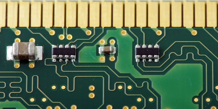
Selective gold plating PCB manufacturing employs controlled electrochemical deposition to apply gold layers exclusively to predetermined circuit areas. The process begins with a chemical nickel barrier layer (2-5 microns) that provides mechanical stability and prevents gold diffusion into the copper substrate, followed by electrolytic gold deposition through precisely controlled current density and solution chemistry. Key parameters include current densities of 0.5-2.0 A/dm², temperature control at 60-65°C, and pH values of 4.2-4.8, with potassium gold cyanide solution concentrations of 8-12 g/L ensuring controllable deposition rates.
Gold layer thicknesses typically range from 0.1-2.5 microns (depending on application requirements), with edge connector gold fingers commonly specified at 1.27-2.54 microns for optimal wear resistance. Brighteners achieve target hardness values of 130-200 HV25, significantly exceeding soft gold specifications. Selective gold plating maintains thickness uniformity within ±20% tolerance through precise agitation control and management of current distribution across different pad sizes in multilayer PCB structures.
Design Optimization Strategies
Strategic design optimization significantly impacts process efficiency and final performance characteristics. Understanding the relationship between circuit geometries, plating distribution, and functional requirements enables engineers to specify optimal solutions for specific applications.
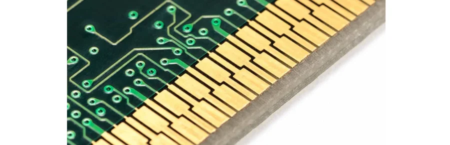
Edge connector applications require careful consideration of contact geometries and gold thickness distribution. Standard gold fingers require 45° beveling (0.8-1.0mm width), while high-frequency PCB applications may specify 30° beveling for improved impedance control. Contact finger spacing maintains minimum 0.5mm gaps to prevent plating solution bridging during processing.
Modern designs increasingly specify gold plating in via-in-pad and fine-pitch component areas. Via-in-pad applications benefit from selective gold deposition, particularly in HDI PCB designs where filled microvias require reliable electrical connections. Gold thicknesses on these features typically range from 0.1-0.5 microns, sufficient to provide oxidation protection while maintaining solderability.
The technique is critical in rigid-flex PCB applications where rigid-to-flex transition areas experience repeated mechanical stress. Gold plating in these interconnection zones provides superior durability compared to alternative finishes, with typical thicknesses of 0.75-1.25 microns optimizing flexibility and connection reliability.
Design guidelines recommend: minimizing pad sizes to functional requirements, consolidating gold-plated areas where possible, and specifying thicknesses based on actual wear expectations rather than conservative maximums. This approach achieves significant cost optimization while maintaining performance requirements.
Cost-Benefit Analysis and Economic Optimization
Optimizing the economics of selective gold plating production requires balancing material costs, process complexity, and performance requirements across applications:
- Material Cost Impact: Gold material represents 60-80% of selective plating costs. Area optimization is critical for cost-effective production, with gold coverage areas <15-20% being more economical than full-board plating.
- Cost Comparison: While selective plating requires additional masking operations (increasing labor/material costs), total costs remain lower. These additional costs typically represent 10-15% of total plating costs, easily offset by material savings.
- Return on Investment (ROI): ROI assessment must consider direct material costs and long-term operational benefits. For wear-prone connectors, environmental exposure, or critical electrical contacts, selective plating costs are frequently offset by reduced warranty claims and extended service life.
- Lifecycle Analysis: Comparative studies show automotive applications with selective gold plated PCBs experience 75-85% fewer field failures than alternative finishes under identical conditions. Medical devices similarly demonstrate reliability improvements.
- Volume vs. Complexity: Economics vary significantly with production volume and board complexity. Utilizing turnkey assembly services can further optimize costs.
Selective Gold Plating Technology Leadership
HILPCB employs laser direct imaging resist systems achieving <50 micron feature accuracy, supporting gold plating requirements for ultra-fine pitch components and high-density interconnects. Our automated production lines integrate solution monitoring, current control, and quality inspection, ensuring continuous optimization.
Why Choose HILPCB?
HILPCB offers unmatched expertise in selective gold plating, delivering high-performance solutions across industries. Whether you're working in 5G infrastructure, electric vehicles, or other advanced fields, we ensure your PCBs meet the highest standards for high-frequency performance, reliability, and environmental durability.
FAQs About Selective Gold Plating PCB
What is the difference between hard gold and soft gold plating?
Hard gold (Type I) contains cobalt or nickel additives (0.1-0.3%) that increase hardness to 130-200 HV25, making it ideal for wear applications like edge connectors. Soft gold (Type III) is pure (99.9%+) with hardness values of 60-90 HV25, preferred for wire bonding applications due to superior bondability. Hard gold offers 5-10x greater wear resistance but slightly higher contact resistance compared to soft gold.
How does selective gold plating compare to ENIG for fine-pitch components?
Selective gold plating offers superior performance for fine-pitch components requiring repeated mating cycles or environmental exposure. While ENIG provides adequate protection with 0.05-0.1 microns of immersion gold, selective plating delivers 0.5-2.5 microns of electrolytic gold with superior wear characteristics. For one-time assembly applications, ENIG remains cost-effective, but selective plating excels where mechanical durability is critical.
What quality control measures ensure reliable selective gold plating?
Our quality control protocol includes:
- XRF thickness measurement at multiple board locations ensuring ±20% thickness uniformity
- Adhesion testing via tape test (ASTM D3359) and thermal shock cycling
- Solderability verification through wetting balance testing
- Contact resistance measurement (<10 mΩ for gold-to-gold contacts)
- Wear resistance validation through mating cycle testing (typically 500-1000 cycles)
- Visual inspection for plating defects, discoloration, or contamination
Contact HILPCB today for expert guidance on selective gold plating solutions for your advanced PCB applications.