As the demand for thinner, lighter, and more cost-effective electronics grows, single layer flex PCBs have become the most practical solution for simple yet reliable interconnections. At HILPCB, we are a full-service PCB manufacturer in China providing end-to-end fabrication of single layer flexible printed circuits — from design optimization and prototyping to mass production and turnkey PCB assembly.
Our single-sided flexible circuits are widely used in LED lighting, sensor systems, wearable devices, battery modules, and automotive electronics, offering an ideal balance of flexibility, performance, and cost. With in-house capabilities for rigid, flexible, rigid-flex, ceramic, and glass PCB manufacturing, HILPCB ensures unified process control, faster delivery, and consistent quality across all circuit types.
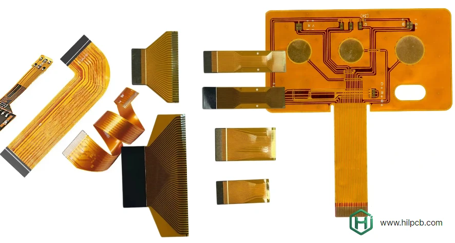
What Is a Single Layer Flex PCB?
A single layer flex PCB (also called a single-sided flexible circuit) features one conductive copper layer bonded to a flexible dielectric substrate such as polyimide (PI) or polyester (PET). The circuit is protected by a flexible coverlay or solder mask, with component pads selectively exposed for assembly. This simple structure results in superior flexibility, lower cost, and faster production compared to multilayer PCB designs.
Key Construction Elements
- Flexible Base Substrate: Polyimide for high reliability, or polyester for budget-friendly applications.
- Copper Layer: 0.5oz to 1oz copper, electrodeposited for standard circuits or rolled annealed for dynamic flex PCB designs.
- Coverlay Protection: Polyimide film or flexible solder mask with selective openings.
- Stiffeners: FR4 PCB or polyimide stiffeners reinforcing connector and component areas.
This minimal layer count simplifies manufacturing, improves yield, and allows custom shapes — perfect for compact, lightweight electronics.
Single Layer Flex PCB Manufacturing Process
At HILPCB, our automated flex PCB production line ensures precision, cleanliness, and repeatability through every stage.
Fabrication Workflow
- Material Preparation: Controlled storage, surface cleaning, and thermal stabilization of films.
- Photo-Patterning & Etching: Laser direct imaging and precision etching create clean, accurate circuits with ±25 μm tolerance.
- Coverlay Application: Vacuum lamination and alignment inspection prevent air bubbles and ensure adhesion.
- Cutting & Profiling: Laser or die-cutting achieves complex outlines for high-volume production.
- Final Inspection: AOI and electrical testing verify continuity, isolation, and dimensional accuracy.
Our optimized processes reduce lead time by up to 30% compared to typical flex PCB suppliers in China.
Common Applications of Single Layer Flex PCBs
LED and Display Electronics
- Flexible LED strip and backlight interconnects.
- Compact design for thin LCD/OLED panels.
- High thermal PCB materials improving heat dissipation.
- Ideal for signage, automotive lighting, and consumer lighting products.
Battery and Sensor Systems
- Flexible connections between battery modules and mainboards.
- Power and signal transfer with vibration isolation.
- Chemical-resistant and biocompatible for industrial or medical sensors.
- Supports compact energy storage systems and smart devices.
Wearable and Medical Devices
- Ultra-thin circuits for comfort and ergonomic design.
- Polyimide and biocompatible coatings for skin contact safety.
- Seamless integration with flex PCB assemblies.
- Used in smartwatches, health trackers, and diagnostic patches.
Design Guidelines for Single Layer Flex Circuits
Electrical and Mechanical Optimization
- Minimum trace width: 0.10 mm (4 mil)
- Minimum spacing: 0.10 mm (4 mil)
- Copper thickness: 18–35 μm depending on current load
- Bend radius: ≥ 6–10× total thickness (static)
Rounded corners, teardrop vias, and evenly distributed traces enhance flexibility and reduce stress cracking. Avoid vias and heavy copper areas in bend zones for best performance.
Component and Connector Design
- Use stiffeners under SMT areas to prevent warping.
- Choose finishes like ENIG for fine-pitch pads or hard gold for contact fingers.
- Keep components 3–5 mm away from bend lines.
- Evaluate soldering temperature limits for polyimide films.
Material Selection and Cost Optimization
Material choice directly impacts price and performance. HILPCB helps engineers balance cost, flexibility, and thermal stability.
| Material | Recommended Use | Cost Impact |
|---|---|---|
| Polyimide (PI) | High-reliability, high-temp applications | ★★★★ |
| Polyester (PET) | Consumer electronics, short flex life | ★★ |
| Rolled Annealed Copper | Dynamic flex or continuous bending | ★★★★ |
| ED Copper | Static applications, LED lighting | ★★ |
We offer both adhesive-based and adhesiveless laminates — adhesiveless options reduce thickness and improve bending life, while adhesive-based materials minimize cost.
Lead Time and Production Options
- Prototypes (1–50 pcs): 5–7 working days
- Low Volume (100–500 pcs): 10–12 working days
- Mass Production: 15–20 days, with large volume assembly available
- Quick Turn Express: 3–5 days for urgent projects
Tooling-free laser cutting and digital prototyping make early design validation fast and affordable.
Quality Control and Certifications
All single layer flex PCBs are built under strict quality standards:
- ISO 9001:2015, ISO 13485, IATF 16949 certified facility
- IPC-6013 & IPC-A-610 Class 3 compliance
- 100% electrical testing and AOI inspection
- Peel strength, humidity, and thermal shock reliability testing
Our process traceability ensures full documentation for medical, aerospace, and automotive customers.
Why Choose HILPCB as Your PCB Manufacturing Partner
Choosing HILPCB means partnering with a one-stop PCB factory capable of producing all board types — from single layer flex and rigid-flex PCBs to ceramic, glass, and high-frequency boards. By keeping fabrication, assembly, and testing under one roof, we reduce communication delays, improve consistency, and optimize cost per unit.
Whether you need low-cost flexible circuits or complex hybrid PCB assemblies, HILPCB delivers precision manufacturing, fast lead times, and long-term reliability trusted by global OEMs.
Frequently Asked Questions — Single Layer Flex PCB
Q1: What’s the difference between single layer and double layer flex PCBs?
Single layer flex uses one conductive layer, ideal for simple interconnections.
Double layer flex PCB adds routing flexibility and ground planes for higher-density designs.
Q2: What’s the minimum bend radius for single layer flex PCBs?
Typically 6–10× total thickness for static bends, and 10–15× for continuous motion.
Q3: Can single layer flex circuits support SMT components?
Yes — with stiffeners under component areas and proper SMT assembly support fixtures.
Q4: What is the typical cost range?
Single layer flex PCBs are 40–60% cheaper than multilayer or rigid-flex PCB equivalents, depending on material and copper weight.
Q5: What industries use single layer flex PCBs most?
LED lighting, consumer electronics, medical sensors, automotive interiors, and wearables all rely on single layer flex circuits for cost-effective interconnect solutions.