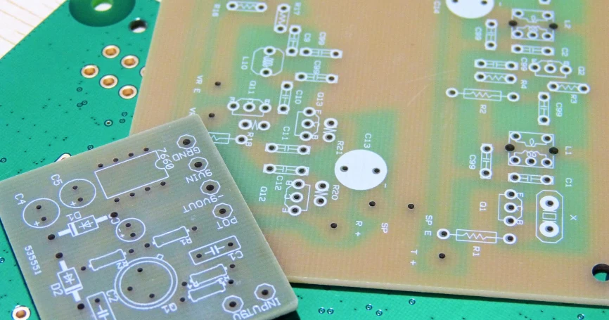
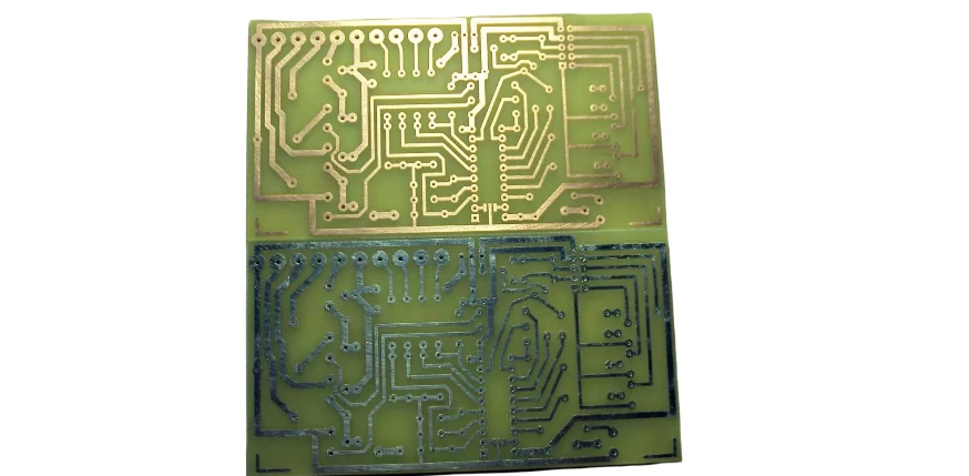
A single layer FR4 PCB (single-sided PCB) has one copper layer on an FR4 substrate. It’s the most economical choice for simple analog, power, lighting, and educational electronics. This guide explains the core specs, manufacturing tolerances, and design rules so you can decide when a single-sided board offers the best value—and when to upgrade to a double layer FR4 PCB.
Core Technical Specifications
Single-sided FR4 boards are simple, but good engineering outcomes still rely on material data and realistic tolerances.
FR4 Material (Typical)
- Dielectric constant (Dk): 4.2–4.8 @ 1 MHz
- Loss tangent (Df): ~0.02 @ 1 MHz
- Glass transition temperature (Tg): 130–140 °C (standard); 170 °C+ available
- Thermal conductivity: ~0.3–0.4 W/m·K
- Moisture absorption: < 0.15%
Copper Foil
- Common thickness: 1 oz (≈35 µm); 2 oz (≈70 µm) optional
- Conductivity: ~5.8 × 10^7 S/m
- Peel strength: ≥ 1.5 N/mm (proper prep and curing)
Manufacturing Tolerances (Typical Capability)
| Parameter | Standard | Precision |
|---|---|---|
| Board outline | ±0.20 mm | ±0.10 mm |
| Hole diameter | ±0.10 mm | ±0.05 mm |
| Hole position | ±0.15 mm | ±0.08 mm |
| Trace width | ±20% | ±10% |
| Copper thickness | ±10% | ±5% |
Design Considerations and Limitations
Current Carrying & Thermal
Use IPC-2152 methodology (or your preferred calculator) to size traces with adequate temperature rise margins. Practical guidance:
- Heavier copper (e.g., 2 oz) supports higher currents and reduces temperature rise.
- Wider traces on a single layer are straightforward—no via constraints.
- Apply copper pours to improve heat spreading; consider ambient derating and airflow.
Routing Strategies (No Second Layer)
- Jumper solutions: Zero-ohm resistors or wire links to cross traces when necessary.
- Placement-first: Group related circuits to minimize crossings and trace length.
- Component-as-bridge: Bodies can help “step over” short runs in low-voltage sections.
- Keepouts: Plan keepouts around mechanicals and large through-hole pads to avoid choke points.
EMI & Grounding
- Favor short return paths and star grounds for analog sections.
- For switching supplies or clocks, keep loops tight; if noise margins are tight or frequency > ~10 MHz, consider stepping up to a double layer FR4 PCB or multilayer FR4 PCB.
Cost Advantages of Single Layer FR4 PCB Manufacturing
A single layer FR4 PCB is the most cost-efficient option for simple and low-to-medium complexity designs. Its manufacturing process eliminates multiple lamination and alignment steps required in multilayer boards, resulting in lower tooling and production costs.
Why Single Layer FR4 PCBs Are More Affordable
- No interlayer registration – Only one copper layer simplifies imaging and exposure.
- Higher panel utilization – Efficient layout reduces material waste and improves yield.
- Simpler process flow – Fewer production stages mean faster turnaround and reduced setup time.
- Lower tooling cost – Single-sided panels require minimal drilling and alignment fixtures.
By reducing both process complexity and cycle time, single layer FR4 PCBs deliver excellent cost-to-performance balance for power circuits, LED boards, and basic control systems.
Standard Process Flow
- Material prep: FR4 sheet with copper foil
- Drilling: Through-holes and mounting features
- Imaging: Photoresist application & exposure
- Etching: Pattern copper to form circuits
- Solder mask: Apply color (e.g., black FR4 PCB or other)
- Silkscreen: Reference and polarity marks
- Finish: HASL, ENIG, or OSP per design needs
- Routing/Depanel: CNC or V-score as required
- Testing: Electrical verification (flying probe/fixture)
Why Choose HILPCB for Single Layer PCB Manufacturing
When you design a single layer FR4 PCB, HILPCB turns your design into a finished product — exactly as specified, with reliable quality and color consistency. If you can design it, we can manufacture it.
What Sets HILPCB Apart
- Full design compatibility – We accept all standard Gerber and manufacturing formats. Any design that meets PCB layout standards can be produced accurately.
- Stable quality control – Every board passes automated optical inspection (AOI) and electrical testing to ensure zero open or short circuits.
- Flexible order sizes – From one prototype to large-volume runs, we maintain the same process precision and delivery reliability.
- Custom solder mask colors – Choose from red, blue, green, yellow, black, white, or any custom Pantone shade.
- Fast lead times – Streamlined production and strong supply chain support short turnaround without compromising quality.
- Consistent results – Whether it’s one panel or a thousand, color tone, copper thickness, and solder mask alignment stay uniform.
HILPCB provides dependable single layer FR4 PCB manufacturing for engineers who need accuracy, flexibility, and confidence. For more advanced circuits, explore our multilayer FR4 PCB options or premium FR4 PCB materials for tighter tolerances and enhanced performance.
FAQ: Single Layer FR4 PCB
Q1: How do I size traces for current on a single-sided board?
Use an IPC-2152-based calculator with your allowed temperature rise, copper weight, and environment. When in doubt, increase width or move to 2 oz copper.
Q2: Can I do fine-pitch SMD on single-sided PCBs?
Yes, within reason. Check the min trace/space above and keep critical nets short. If routing becomes congested, upgrade to a double layer.
Q3: Which surface finish is best?
HASL is cost-effective; ENIG offers flat pads and better corrosion resistance for fine-pitch or long storage; OSP is good for budget and RoHS.
Q4: Can HILPCB match my brand color?
Yes. We support custom solder mask colors in addition to all standard options. Provide a Pantone reference to ensure consistency across batches.