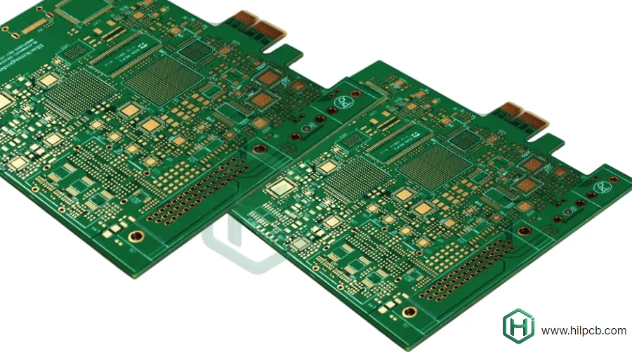
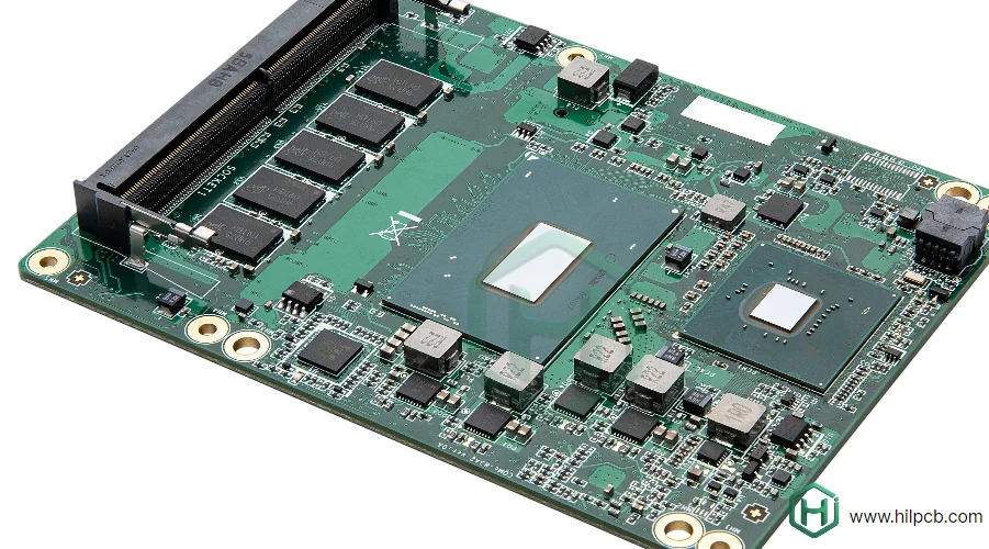
Telecommunications PCBs are the backbone of modern network devices, from base stations to routers and optical transport systems. These systems require high-speed, high-frequency, and low-loss PCBs to meet rigorous performance standards and reliability demands over 10-20 years.
Our Telecommunications PCB solutions provide the precision, durability, and performance required for these critical systems. Whether it’s 5G infrastructure, fiber-optic transport, or network routers, we deliver comprehensive manufacturing services that meet the most demanding specifications.
Why Telecommunications PCBs Are Critical
Telecommunications systems must ensure carrier-grade reliability with continuous operation under harsh environmental conditions. This makes telecom PCB design highly specialized.
Key Requirements for Telecom PCBs
Reliability and Longevity: Telecom equipment is expected to operate 24/7 for decades. Our PCBs are designed to meet 99.999% uptime standards with redundant designs, component derating, and robust thermal management.
Environmental Resistance: Telecom gear operates in a wide range of conditions from outdoor installations (exposure to temperature extremes, humidity, UV) to indoor environments (dust, vibration, 24/7 operation).
High-Speed Data: Telecom systems handle high-speed data and must support protocols such as 100GbE, 400GbE, and optical transport. Our high-speed PCBs ensure high-performance, low-loss data transmission.
Ensuring High-Speed and Low-Loss Performance
To meet high data throughput and low-latency demands, telecom PCBs need precise signal integrity.
Signal Integrity
SerDes (Serializer/Deserializer) interfaces operate at speeds exceeding 10-56 Gbps per lane. We ensure that PCB design maintains controlled impedance and minimizes signal loss for these high-speed connections.
Material Selection: We utilize low-loss laminates (e.g., Megtron 6, RO4003C) to reduce dielectric loss and maintain signal quality at 10 Gbps and beyond. Our use of multilayer PCBs with controlled impedance and laser-drilled vias ensures reliability across high-speed paths.
Power Distribution
Efficient power distribution networks (PDNs) are critical to prevent power degradation:
- We design multiple copper planes and decoupling capacitors to ensure stable power supply across all components, handling high currents for FPGAs and processors.
- Heavy copper PCBs (3-10 oz) are used to manage power distribution efficiently with minimal resistive loss and thermal rise.
Materials and Construction for Telecom PCBs
Material selection for telecom PCBs impacts electrical performance, reliability, and cost.
Materials for Performance
- Standard FR4: Ideal for non-critical layers like power distribution and low-speed control.
- High-Tg FR4: Provides thermal stability in extreme conditions for outdoor telecom equipment.
- Rogers Materials (RO4000 & RO3000 series): Used for high-frequency applications, ensuring low-loss performance and thermal stability in 5G and RF applications.
Thermal Management
Telecom devices, especially power amplifiers, generate substantial heat. We use materials with higher thermal conductivity:
Metal-core PCBs with aluminum or copper cores (up to 300 W/m·K) are employed to handle high power dissipation in base stations and optical transceivers.
Ceramic-filled materials provide an alternative for high-power designs requiring efficient heat dissipation.
Environmental and Regulatory Testing
Telecommunications equipment must meet rigorous standards for environmental durability and regulatory compliance.
Testing for Harsh Environments
- Thermal Cycling: We test PCBs through 500-1000 cycles from -40°C to +85°C to simulate years of operation.
- Humidity Testing: We subject PCBs to 85°C/85% RH to simulate exposure to moisture and corrosion.
- Vibration and Shock Testing: We perform vibration testing to simulate installation and operational stresses.
Regulatory Compliance
- NEBS (Network Equipment Building Standards): Telecom equipment must meet NEBS Level 3 for environmental and earthquake resistance. We ensure all designs pass thermal, shock, and EMI testing as required.
- EMI/EMC Testing: Our designs comply with FCC, CE, and ETSI standards for radiated emissions and immunity.
Conclusion: Telecom PCB Solutions for Next-Generation Networks
Our telecom PCB solutions are engineered for high performance, reliability, and scalability, supporting the evolving demands of 5G, fiber-optic networks, and other next-gen infrastructures. Whether you're developing base stations, routers, or optical transport systems, our custom PCBs ensure that your devices meet the highest standards of speed, efficiency, and durability.
With expertise in 5G, 100GbE, and DWDM, our manufacturing process guarantees exceptional signal integrity, thermal management, and environmental resilience. We deliver tailored PCBs optimized for power efficiency, electromagnetic compatibility (EMC), and long-term operational reliability, ensuring your network equipment stands up to industry demands.
Partner with us for a comprehensive, end-to-end solution, from initial design to production, with expert support at every stage of your project. We ensure your products meet NEBS, EMI/EMC, and environmental testing requirements for the highest telecom-grade performance.
Request Your Telecommunications PCB Quote today and let us help you build the future of global connectivity.