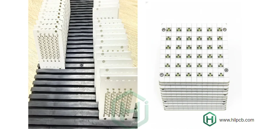
Amid the relentless drive for miniaturization and enhanced performance in electronics, thin film PCB technology has emerged as a cornerstone for high-frequency, precision, and mission-critical circuits. At HILPCB, we specialize in manufacturing thin film PCBs on ceramic and hybrid substrates, delivering high-density, low-loss interconnects essential for aerospace radar, optical communications, RF modules, and advanced medical instrumentation.
What Is a Thin Film PCB?
A thin film PCB is a precision circuit created by depositing metallic traces onto an insulating ceramic, glass, or semiconductor substrate using vacuum deposition techniques like sputtering or evaporation. Unlike traditional PCBs that laminate and etch copper foils, thin film conductors are built up atom by atom into ultra-uniform layers, typically 1 to 10 µm thick. This method enables unmatched fine-line definition, exceptional dimensional stability, and superior electrical performance.
This technology is indispensable when sub-micron accuracy or exceptional high-frequency stability is paramount—such as in microwave filters, photonic sensors, power amplifiers, or implantable medical devices. Compared to conventional PCB manufacturing, thin film circuits deliver:
- Superior impedance control with minimal dielectric variation across the substrate.
- Low conductor surface roughness, significantly reducing signal insertion loss at high frequencies (mmWave).
- Outstanding thermal conductivity, ideal for dissipating heat from power-dense components.
- Vacuum-compatible and radiation-resistant materials, making them suitable for aerospace and space systems.
These features establish thin film PCBs as the backbone of modern RF, optical, and medical electronics, where performance tolerances leave no room for error.
Key Differences: Thin Film vs. Thick Film Circuits
Though both technologies utilize ceramic substrates, thin film and thick film circuits differ fundamentally in their materials, deposition methods, and performance characteristics.
| Feature | Thin Film PCB | Thick Film Circuit |
|---|---|---|
| Conductor Formation | Physical Vapor Deposition (PVD) of pure metals like Au, Pt, Ti, or Cu. | Screen printing of conductive pastes (e.g., Ag, PdAg, Pt) followed by firing. |
| Line Resolution | Capable of ≤10 µm features. | Typically ≥100 µm. |
| Surface Finish | Mirror-smooth and highly uniform. | Rougher surface, dependent on the fired paste composition. |
| Electrical Loss | Extremely low, ideal for high-speed digital and RF applications. | Higher due to surface roughness and binder material resistance. |
| Thermal Stability | Excellent, suitable for aerospace and high-temperature operation. | Good, but limited by the thermal expansion of the glass binder in the paste. |
| Cost and Volume | Higher precision and cost, suited for low-to-medium volume. | Lower cost, ideal for high-volume power hybrid modules and sensors. |
Thin film circuits excel in miniaturized RF modules and precision sensors, whereas thick film technology is dominant in power hybrids, automotive controls, and heater circuits. Many advanced designs integrate both; for instance, using thin film for high-frequency signal routing and thick film for printed resistors on the same ceramic PCB product.
Substrate Materials and Deposition Techniques: A Detailed Overview
The performance of a thin film PCB is intrinsically linked to the choice of substrate material and the precision of the manufacturing process. At HILPCB, we master a wide range of materials and techniques to meet stringent application-specific requirements.
Advanced Substrate Materials
The substrate is the foundation of the circuit, dictating its thermal, mechanical, and electrical behavior.
- Alumina (Al₂O₃): The industry workhorse, Alumina offers a robust balance of mechanical strength, excellent electrical insulation, and good thermal conductivity (~24 W/m·K). Available in various purity grades (e.g., 96% and 99.6%), higher purity yields a smoother surface and lower dielectric loss, making it suitable for higher frequencies.
- Aluminum Nitride (AlN): The premier choice for thermal management, AlN boasts superior heat dissipation (170–200 W/m·K), approaching that of some metals. Its coefficient of thermal expansion (CTE) closely matches silicon, making it ideal for high-power RF devices and direct chip-on-board (COB) assemblies where thermal stress must be minimized.
- Sapphire (single-crystal Al₂O₃): Offering an atomically smooth surface, sapphire is perfect for applications requiring extremely fine lines and controlled optical properties. Its transparency and high dielectric strength make it a top choice for optoelectronics, LEDs, and high-performance microwave circuits.
- Quartz (SiO₂) & Fused Silica: When ultimate high-frequency performance is needed, quartz is unparalleled. It features an extremely low dielectric constant and the lowest loss tangent of common substrates, making it essential for millimeter-wave (mmWave) applications, satellite communications, and precision oscillators.
- Zirconia & Other Dielectrics: Materials like Zirconia are used for their high dielectric strength and robustness in harsh environments, including laser systems and medical-grade sensors.
| Material | Thermal Conductivity (W/m·K) | Dielectric Constant (@1GHz) | Loss Tangent (@1GHz) |
|---|---|---|---|
| Alumina (99.6%) | 24 - 30 | ~9.8 | 0.0001 - 0.0002 |
| Aluminum Nitride | 170 - 200 | ~8.9 | 0.0002 - 0.0005 |
| Sapphire | 35 - 42 | ~9.4 - 11.6 | <0.0001 |
| Quartz (Fused Silica) | ~1.4 | ~3.8 | <0.0001 |
The Thin Film Deposition and Patterning Workflow
Creating thin film circuits is a multi-stage process performed in a pristine cleanroom environment to prevent contamination and ensure precision.
- Substrate Preparation: The process begins with rigorous cleaning of the substrate wafer. This involves ultrasonic baths, solvent rinses, and often plasma etching to remove any organic or particulate contaminants. An atomically clean surface is critical for achieving strong adhesion of the subsequent metal layers.
- Physical Vapor Deposition (PVD): This is the core step where the metal layers are deposited in a high-vacuum chamber.
- Sputtering: An inert gas (like Argon) is ionized to create a plasma. These ions bombard a target made of the desired metal (e.g., Titanium, Gold). The impact dislodges metal atoms, which then travel and deposit onto the substrate, forming a thin, dense, and highly adherent film. Sputtering is excellent for creating adhesion layers (like Titanium or Chromium) before depositing the primary conductive layer (Gold or Copper).
- Evaporation: The source metal is heated in a vacuum until it evaporates. The metal vapor travels in a straight line and condenses onto the cooler substrate. While it can produce very pure films, adhesion is generally less robust than with sputtering.
- Photolithography (Pattern Definition): This process transfers the circuit design from a digital file to the substrate surface.
- Photoresist Coating: A light-sensitive polymer, known as photoresist, is spin-coated onto the metallized substrate to create a uniform layer.
- Exposure: A photomask—a glass plate with an opaque pattern of the desired circuit—is precisely aligned over the substrate. The assembly is then exposed to UV light, which chemically alters the photoresist in the exposed areas.
- Development: The substrate is immersed in a developer solution, which washes away either the exposed (for positive resist) or unexposed (for negative resist) photoresist, revealing the underlying metal in the pattern of the circuit.
- Etching (Pattern Transfer): The circuit pattern is permanently etched into the metal layer.
- Wet Etching: Uses chemical baths to dissolve the unprotected metal. It is fast but isotropic, meaning it etches in all directions, which can cause "undercutting" and limit the minimum feature size.
- Dry Etching (Ion Milling): Uses a focused beam of ions to physically remove the unprotected metal. This process is highly directional (anisotropic), enabling the creation of extremely fine, sharp-edged traces essential for high-frequency performance.
- Resist Stripping and Annealing: The remaining photoresist is chemically stripped away, leaving the final metallic circuit pattern. The wafer may then be annealed (heated in a controlled atmosphere) to relieve stress and further improve film adhesion and stability.
This meticulous, step-by-step process allows HILPCB to achieve the ultra-high precision that defines thin film technology.
Applications in High-Frequency and Medical Devices
Thin film PCBs are critical enablers across industries where signal integrity, miniaturization, and environmental stability are non-negotiable.
RF and Microwave Systems
In 5G transceivers, phased-array antennas, and satellite downconverters, low insertion loss and stable phase performance directly determine system accuracy. The precise impedance control of thin film circuits ensures seamless integration with active components in hybrid microwave modules.
Aerospace and Defense
The ability to withstand vacuum, extreme temperatures, vibration, and radiation makes thin film PCBs the preferred interconnect technology in spacecraft payloads, guidance systems, and advanced radar. Gold-based metallization resists oxidation, ensuring long-term reliability in harsh environments.
Optical and Sensor Electronics
Optoelectronic modules, photodiodes, and spectrometers rely on thin film substrates for precision signal routing and reflective surface control. Their low-profile, planar architecture supports the micron-level alignment required for critical optical components.
Medical Devices and Bioelectronics
Implantable stimulators, diagnostic sensors, and surgical probes leverage thin film circuits for their biocompatibility, potential for hermetic sealing, and long-term reliability. Material stacks like titanium-gold on alumina or sapphire provide both electrical conductivity and corrosion resistance, ensuring safe, stable operation inside the human body.
Power and Hybrid Microelectronics
In power amplifiers and RF drivers, thin film interconnects minimize parasitic losses while the ceramic substrate efficiently dissipates heat. These modules often combine ceramic PCB assembly with thin film signal layers to create compact, thermally-managed System-in-Package (SiP) designs.
Design and Manufacturing Capabilities at HILPCB
HILPCB delivers end-to-end thin film PCB manufacturing—from substrate engineering through patterning, dicing, and final testing—under a single, tightly controlled workflow.
Engineering Capabilities
- Design consultation for impedance matching, thermal management, and trace optimization.
- Multi-layer ceramic structures and thin film–thick film hybrid integration.
- Finite Element Analysis (FEA) for thermal stress and frequency response modeling.
- Customized filled vias and edge metallization for robust interlayer connections.
- Hermetic sealing and packaging for medical or aerospace-grade assemblies.
Fabrication Parameters
- Minimum Line/Space: 75 µm / 75 µm
- Conductor Thickness: 1–15 µm (sputtered + plated)
- Via Diameter: 50–100 µm (laser drilled)
- Alignment Accuracy: ±5 µm (layer-to-layer)
- Surface Finishes: Au, Ni/Au, Ag, or Pt based on application requirements
Quality and Reliability Testing
Every circuit undergoes comprehensive electrical, dimensional, and visual inspection. Environmental validation includes thermal cycling, humidity resistance, and adhesion pull testing to guarantee stable performance across all operating conditions. Our quality systems are certified to ISO 9001, ISO 13485 (Medical Devices), and AS9100 (Aerospace), ensuring our thin film PCBs meet the most demanding industry standards.
Partner with HILPCB for Thin Film PCB Excellence
HILPCB unites advanced ceramic engineering, precision thin film deposition, and deep RF design expertise to deliver high-reliability interconnects that power tomorrow’s most demanding systems.
Whether you need a single-layer alumina circuit or a complex multi-layer AlN hybrid for microwave amplification, we guarantee precision, repeatability, and material integrity at every stage. Our facility integrates thin film processing with downstream assembly, packaging, and testing, providing a complete, turnkey solution that accelerates your product development and time-to-market.
Discover how HILPCB can elevate your high-frequency or medical-grade electronics with our industry-leading thin film PCB technology.