
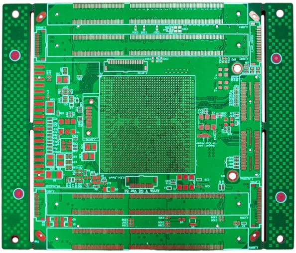
Hochdichte-Verbindungs-PCB-Technologie (HDI) stellt den Höhepunkt der modernen Elektronikfertigung dar und ermöglicht die Schaffung kompakter, leistungsstarker Geräte, die heutige Smartphones, Tablets und fortschrittliche Computersysteme antreiben.
HDI-Technologie verstehen
HDI-PCBs zeichnen sich durch ihre feinen Linien, kleinen Vias und hohe Verbindungspad-Dichte aus. Diese Platinen weisen typischerweise folgende Merkmale auf:
- Mikrovias: Löcher mit Durchmessern ≤ 150μm
- Feinpitch-Komponenten: BGA-Raster bis zu 0,4mm
- Dünne dielektrische Schichten: 25-100μm Dicke
- Hohe Lagenzahlen: Bis zu 20+ Lagen in kompakten Formfaktoren
Manufacturing Process Overview
1. Sequential Lamination Process
The sequential build-up process is fundamental to HDI manufacturing:
Core Layer → Prepreg → Copper Foil → Lamination → Drilling → Plating
Each layer is built sequentially, allowing for precise control of impedance and signal integrity.
2. Micro-via Formation
Laser Drilling Technology
- CO2 lasers: For dielectric materials
- UV lasers: For copper removal
- Plasma desmear: Surface preparation for plating
Via Types in HDI
- Blind vias: Connect outer layer to inner layer
- Buried vias: Connect inner layers only
- Stacked vias: Multiple microvias in alignment
- Staggered vias: Offset microvias for routing flexibility
Advanced Quality Control
Automated Optical Inspection (AOI)
- High-resolution imaging systems
- Pattern recognition algorithms
- Defect classification and reporting
- Real-time process feedback
X-ray Inspection
- Via fill quality assessment
- Hidden defect detection
- Layer alignment verification
- Component placement validation
Electrical Testing
- In-Circuit Testing (ICT): Continuity and isolation
- Flying Probe Testing: Flexible test point access
- Boundary Scan: Digital circuit verification
Material Considerations
Substrate Materials
- Low-loss dielectrics: For high-frequency applications
- Thermally conductive materials: For heat dissipation
- Low CTE materials: Dimensional stability
Copper Foil Selection
- Ultra-thin copper: 9μm and 12μm foils
- Low-profile copper: Reduced surface roughness
- Treated copper: Enhanced adhesion properties
Design Guidelines for HDI
Via Design Rules
- Minimum via size: 100μm (4 mil)
- Via-to-via spacing: 150μm minimum
- Via-to-trace spacing: 75μm minimum
- Annular ring: 25μm minimum
Trace and Space Requirements
- Minimum trace width: 75μm (3 mil)
- Minimum spacing: 75μm (3 mil)
- Impedance tolerance: ±10%
Applications and Benefits
Consumer Electronics
- Smartphones and tablets
- Wearable devices
- Ultra-thin laptops
- Gaming consoles
Industrial Applications
- Medical devices
- Automotive electronics
- Aerospace systems
- IoT devices
Performance Advantages
- Size reduction: Up to 70% smaller than conventional PCBs
- Weight reduction: Lighter form factors
- Improved signal integrity: Shorter signal paths
- Enhanced thermal performance: Better heat dissipation
Manufacturing Challenges and Solutions
Challenge: Via Reliability
Solution: Optimized drilling parameters and advanced plating chemistry
Challenge: Layer Registration
Solution: High-precision lamination equipment with vision systems
Challenge: Yield Optimization
Solution: Statistical process control and real-time monitoring
Future Trends in HDI Technology
Emerging Technologies
- Any-layer HDI: Vias connecting any layer combination
- Embedded components: Passive components within PCB layers
- 3D printing integration: Additive manufacturing techniques
- Advanced materials: Liquid crystal polymers and ceramics
Industry 4.0 Integration
- IoT-enabled manufacturing equipment
- Predictive maintenance systems
- AI-driven quality control
- Digital twin technology
Quality Standards and Certifications
International Standards
- IPC-2226: HDI design guidelines
- IPC-6016: HDI qualification standards
- IPC-A-600: Acceptability criteria
- ISO 9001: Quality management systems
Testing Protocols
- Thermal cycling: -55°C to +125°C
- Humidity testing: 85°C/85% RH
- Mechanical stress testing
- Accelerated aging tests
Häufig gestellte Fragen
Wodurch unterscheidet sich die HDI-PCB-Fertigung von der Herstellung herkömmlicher Multilayer-Leiterplatten?
Die HDI-Fertigung arbeitet mit feineren Leiterbahnen, kleineren Vias, dünneren Dielektrika und sequenziellen Aufbauprozessen, die eine deutlich engere Prozesskontrolle verlangen. Hinzu kommen Laserbohren, fortschrittliche Galvanik und strengere Registrierungsanforderungen.
Warum sind Microvias bei HDI-Platinen so wichtig?
Microvias verkürzen Routing-Wege und ermöglichen die Anbindung dichter Fine-Pitch-Bauteile, ohne zu viel Fläche zu verbrauchen. Sie sind für kompakte Designs entscheidend, stellen aber hohe Anforderungen an Bohren, Desmear, Metallisierung und Zuverlässigkeit.
Welche Prüfungen sind für die HDI-Qualitätssicherung am wichtigsten?
AOI, Röntgeninspektion und elektrische Tests sind alle wesentlich, weil jede Methode andere Risiken aufdeckt. AOI erkennt Oberflächenfehler, Röntgen zeigt verborgene Strukturprobleme, und elektrische Tests bestätigen Durchgang und Isolation der fertigen Platine.
Wann sollte ein Entwicklungsteam HDI statt eines Standard-Stack-ups wählen?
HDI ist meist sinnvoll, wenn das Design Fine-Pitch-BGAs, hohe I/O-Dichte, enge Platzgrenzen oder kurze Hochgeschwindigkeitsverbindungen enthält. Wenn ein konventioneller Aufbau das Routing nicht mehr sauber lösen kann oder das Produkt zu groß machen würde, ist HDI gerechtfertigt.
Conclusion
Advanced HDI PCB manufacturing represents a critical capability for companies seeking to develop next-generation electronic products. The combination of precision manufacturing techniques, advanced materials, and rigorous quality control enables the creation of high-performance, reliable electronic assemblies.
At Highleap PCB, our investment in state-of-the-art HDI manufacturing equipment and processes ensures that we can meet the most demanding requirements for modern electronics applications.
For technical specifications and custom HDI solutions, contact our engineering team for a comprehensive consultation.