
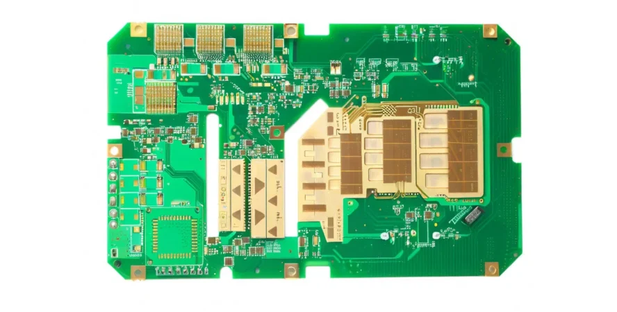
Im Zentrum von AI und HPC hängen Performance-Sprünge von tiefen Hardware-Innovationen ab. HBM3 ist ein Schlüssel, um die Memory Wall zu durchbrechen. Doch die Brücke zwischen GPU/TPU und HBM3 Stacks—Interposer und das organische Substrate PCB—steht unter extremem Reliability-Druck. Als Engineer für Mass-Production Validation weiß ich: HBM3 interposer PCB reliability entscheidet, ob teure AI Accelerators im Data Center über Jahre stabil laufen.
2.5D/3D Packaging Module liegen oft bei 1000W+ und TB/s Datenrate. Unter solchen Bedingungen eskalieren kleine Design-/Material-/Process-Fehler schnell zu System Failures. Deshalb ist das systematische Lösen von HBM3 interposer PCB reliability die Basis für End-to-End Erfolg von Design über Manufacturing bis Validation. Hersteller wie Highleap PCB Factory (HILPCB) unterstützen mit Advanced Processes und strikter QC.
Was treibt die Reliability-Challenges von HBM3 Interposer PCBs fundamental?
HBM3 Interposer PCBs sind nicht “normale PCBs”, sondern der Schnittpunkt von Packaging und System Interconnect—oft in CoWoS (Chip-on-Wafer-on-Substrate). Logic Die (GPU) und HBM Stacks sitzen auf einem Silicon Interposer und werden dann auf ein High-Performance Organic Substrate verpackt.
Daraus entstehen drei Kernquellen:
Thermomechanical Stress: hoher TDP → extreme Heat Flux. Unterschiedliche Materialien (Silicon, Copper, Organic, Solder) haben stark unterschiedliche CTE. Power Cycling erzeugt große Interface-Stresses → Cracks/Delamination.
Electrical Performance Demands: tausende I/O, 6.4 Gbps+ pro Channel. Mikrometer-Strukturen sind extrem sensibel gegenüber Impedance, Crosstalk und Power Noise. Kleine Degradation kann BER erhöhen → Electrical Reliability Problem.
Manufacturing Process Limits: Line/space bis ~10µm und stacked Microvias. Das fordert extreme Precision/Consistency. Plating Non-uniformity, Misregistration, Lamination Defects sind latent Risks.
Wie thermomechanical Stress die Interposer-Integrity “abrieben” kann
Thermal Cycling ist Kern der Long-Term Reliability Validation (z. B. JEDEC -40°C…125°C), um Schwächen zu beschleunigen.
Häufige Failure Modes:
- Microvia cracking: CTE Mismatch zwischen Copper Plating und Dielectric erzeugt Stress Concentration; Fatigue Cracks → Opens, besonders kritisch bei stacked microvias.
- Pad Cratering: Stress unter BGA Pads kann Resin Cracks verursachen—schwer zu detektieren.
- Delamination: schlechte Adhesion + Moisture Ingress → Interface Separation; SI und Thermals leiden.
Für Mitigation sind High Tg und Low Z-axis CTE High Tg PCB Materials zentral.
Key thermomechanical failure modes and mitigation strategies
| Failure mode | Root cause | Design/manufacturing mitigations |
|---|---|---|
| Microvia cracking | Copper fatigue from CTE mismatch | Optimize microvia structure (copper fill), control plating ductility, select low-CTE materials |
| Pad cratering | Stress concentration under pads | Use NSMD design, improve resin toughness |
| Delamination | Low adhesion + moisture ingress | High-adhesion materials, strict lamination control, thorough bake before shipment |
Warum HBM3 interposer PCB impedance control keinen Spielraum hat
Bei HBM3 wird jede Trace zur Präzisions-Transmission-Line. HBM3 interposer PCB impedance control ist deshalb existenziell.
Mismatch erzeugt Reflections; diese schließen das Eye und erhöhen Fehlinterpretationen. Bei 1024-bit Interface kann ein einzelner intermittierender Channel das System crashen.
Für präzise Impedance Control braucht es Co-Design:
- Design: Field Solver mit Dk/Df, Width, Dielectric Thickness, Reference Spacing.
- Manufacturing: Kontrolle von etched Width, Dielectric Thickness, Dk/Df Consistency. Toleranz oft ±5%—eine harte Forderung auf IC substrate PCB Level.
Hersteller wie HILPCB nutzen TDR für Sample/Full Inspection pro Lot.
Core Principles für robustes HBM3 interposer PCB design
Robuste PCBs entstehen aus System Design. Dieses HBM3 interposer PCB guide fasst Kernprinzipien:
Symmetric/balanced stackup: Asymmetrie führt zu Warpage in Reflow und gefährdet Die Attach/Assembly.
PDN excellence: Low-Impedance Planes, Decaps nahe Pins, Inductance-Loop Control gegen IR Drop und Power Noise.
No-compromise SI:
- Reference continuity: kontinuierliche Reference Planes unter High-Speed Nets.
- Crosstalk control: 3W Spacing als Basis.
- Via optimization: Vias minimieren; Backdrill gegen stub.
Gutes HBM3 interposer PCB design balanciert Performance, Cost, Manufacturability. Early DFM mit HILPCB reduziert spätere Redesigns.
Interposer substrate material comparison
| Metric | Standard FR-4 | High Tg FR-4 | ABF-like build-up materials | Reliability impact |
|---|---|---|---|---|
| Tg | ~140°C | >170°C | >200°C | Higher Tg improves dimensional stability and delamination resistance. |
| CTE (Z-axis, ppm/°C) | 50-70 | 40-60 | <40 | Lower CTE reduces mismatch to silicon/copper and stress. |
| Dk (@10GHz) | ~4.5 | ~4.2 | <3.5 | Lower Dk improves speed and reduces crosstalk. |
| Df (@10GHz) | ~0.020 | ~0.015 | <0.005 | Lower Df reduces attenuation—critical for [High Speed PCB](/products/high-speed-pcb). |
HBM3 interposer PCB routing und Reliability
HBM3 interposer PCB routing ist High-Density Engineering: tausende High-Speed Nets plus Power/GND in kleinem Footprint.
- Escape Routing: µBGA Breakout via HDI + Microvias direkt aus Pads.
- Length Matching: DQS/DQ Längen strikt matchen; Serpentines erhöhen Complexity.
- No sharp corners/stubs: 45°/Arc statt 90°; keine Stubs als Reflection Sources.
Komplexes Routing braucht EDA Tools + Erfahrung. Schlechte Planung kann sogar Acid Traps erzeugen und Etch Quality/Reliability schädigen.
Was macht eine industrial-grade HBM3 interposer PCB aus?
Eine industrial-grade HBM3 interposer PCB muss Jahre 7x24 laufen. Das fordert:
- Core materials: ABF oder vergleichbare Build-up Dielectrics (low Dk/Df, high temp, low CTE, laser drill friendly).
- Manufacturing precision: 15/15µm oder feiner, tight registration, plating uniformity.
- Reliability validation: HAST, TCT, mechanical shock/vibration.
HILPCB IC substrate-level manufacturing capabilities
| Parameter | HILPCB capability | Parameter | HILPCB capability |
|---|---|---|---|
| Max layers | 32 Layers | Min line/space | 1.0/1.0 mil (25/25 µm) |
| Board thickness | 0.2 - 3.2 mm | Min mechanical drill | 0.1 mm |
| Min laser microvia | 50 µm | Impedance tolerance | ±5% |
| Supported materials | ABF, BT, High Tg FR-4 | Surface finish | ENEPIG, Immersion Tin/Silver |
Mandatory manufacturing processes and defect controls
- Build-up Process: precise temperature/pressure/vacuum to avoid delamination/voids.
- Laser Drilling: energy/spot/focus define via quality.
- Copper Filling: void-free fill via chemistry/current control.
- AOI/AXI: AOI for surface defects; AXI for internal connectivity.
In production, SPC monitoring plus DPA (microsections) keep processes under control.
HILPCB end-to-end reliability for AI programs
HILPCB ensures HBM3 interposer PCB reliability with:
- Design collaboration via DFM/DFA to optimize HBM3 interposer PCB design.
- Top-tier materials/processes including ABF expertise.
- Full QA (IQC/IPQC/FQC) + AOI/AXI/TDR + reliability testing.
- Turnkey manufacturing and assembly via SMT Assembly and Turnkey Assembly.
Fazit
HBM3 interposer PCB reliability ist der ultimative End-to-End Test: Thermomechanical Stability, Electrical Integrity und Manufacturing Excellence. Mit steigender AI-Performance steigen die Anforderungen weiter.
Wer Interposer-Reliability ignoriert, baut auf wackeligem Fundament. Mit Failure-Mechanism Understanding, robusten Design-Prinzipien und einem Partner wie HILPCB können Sie diese Challenges meistern und Ihr Produkt wettbewerbsfähig halten. Kontaktieren Sie uns für High-Reliability AI Interconnect Solutions.