Accurate data preparation is critical to transforming a PCB design into a manufacturable product. This guide explains how CAM files serve as the bridge between your design software and the physical manufacturing process. By understanding how these files work-and how CAM engineers optimize them-you can avoid costly production errors, improve fabrication efficiency, and ensure your boards meet all design and quality specifications.
What Are CAM Files and Why Do They Matter in PCB Manufacturing?
CAM (Computer-Aided Manufacturing) files translate your PCB design data-typically in Gerber or ODB++ formats-into precise manufacturing instructions for fabrication and assembly. They ensure that every drill hole, trace width, and copper layer in your design is correctly interpreted by the machines on the factory floor.
The Role of CAM Engineers
CAM engineers validate and prepare these files to ensure manufacturability. Their tasks include running design rule checks (DRC), performing panelization, and resolving data inconsistencies such as trace violations or misaligned drill holes. Essentially, CAM engineers act as the bridge between design and production, making sure your board can be fabricated accurately and efficiently.
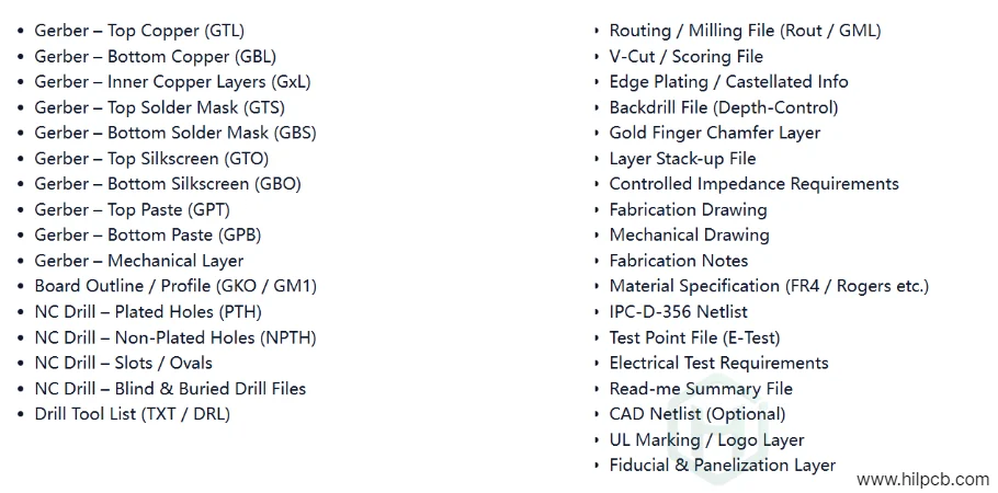
Key Components of CAM Files in PCB Manufacturing
In modern PCB manufacturing, CAM (Computer-Aided Manufacturing) files serve as the bridge between digital circuit design and physical board production. Each file type within the CAM package provides unique data essential for accurate fabrication and assembly. Understanding these components ensures your PCB is manufactured with precision, consistency, and high yield.
At HILPCB, our engineering team reviews and optimizes every layer of the CAM file package - from Gerbers to drill data - ensuring manufacturability, electrical reliability, and cost efficiency for both prototype and mass production boards.
1. Gerber Files
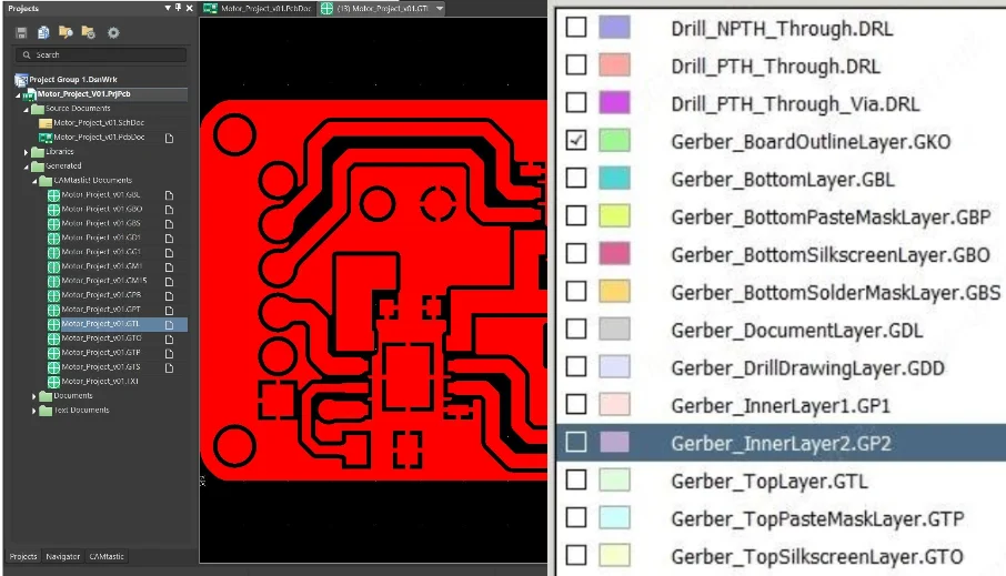
Gerber files form the core of every PCB manufacturing process. They define the copper circuitry, solder mask, silkscreen, and mechanical outlines of each board layer. Each layer of the PCB design corresponds to one Gerber file.
- Copper Layers: Represent all signal traces, pads, and ground planes.
- Solder Mask Layers: Protect copper from oxidation and prevent solder bridging.
- Silkscreen Layers: Include text, component IDs, logos, and polarity markings.
- Mechanical Layers: Define outlines, slots, keep-outs, and fiducials for assembly.
A complete Gerber set ensures the manufacturer can reproduce the exact electrical and mechanical layout intended by the designer.
2. Drill Files
Drill files specify the size, location, and type of every hole on the PCB, enabling accurate component placement and inter-layer connectivity. These files are typically generated in Excellon format, the industry standard for CNC drilling machines.
Common drill types include:
- Through Holes: Extend through all PCB layers, used for vias or through-hole components.
- Blind Vias: Connect outer layers to one or more inner layers without penetrating the entire stack.
- Buried Vias: Located entirely within inner layers, ideal for high-density multilayer designs.
- Countersunk Holes: Allow screw heads to sit flush with the PCB surface, improving assembly fit.
- Tapered Holes: Designed for components requiring a conical entry or exit geometry.
- Back Drilled Holes: Remove unused via stubs in high-speed boards to improve signal integrity.
In addition, hole tolerance specifications (e.g., ±0.05 mm) are included to ensure accurate fit and alignment during component insertion and plating. Properly defined tolerances help prevent mechanical stress, poor solder joints, and misalignment during PCB assembly.
3. Pick-and-Place Files
For PCB assembly, pick-and-place files are essential. They instruct automated assembly machines where and how to position each component.
- Component Coordinates (X/Y): Define the exact position of each part.
- Rotation Data: Ensures correct orientation for polarized and directional components.
- Side Indication: Specifies whether components are on the top or bottom layer of the PCB.
Accurate pick-and-place files minimize placement errors, reduce assembly time, and improve yield during high-volume production.
4. Bill of Materials (BOM)
The Bill of Materials lists every component required for PCB assembly. It includes part numbers, package types, quantities, and sourcing information.
- Manufacturer Part Numbers (MPNs): Ensure consistent component sourcing.
- Component Values: Define resistances, capacitances, and ratings.
- Supplier References: Facilitate procurement and replacement planning.
A precise BOM supports efficient component sourcing, assembly verification, and traceability for quality control.
5. Mechanical & Fabrication Layers
Mechanical layers define the physical characteristics of the PCB beyond its electrical design. These details ensure compatibility with enclosures, connectors, and mounting hardware.
- Board Outline & Cutouts: Define final dimensions and special shapes.
- Mounting Holes & Slots: Guide mechanical integration with casings or chassis.
- Keep-Out Areas: Prevent copper placement near edges or mounting zones.
- Panelization Data: Shows how multiple boards are arranged for efficient production.
Combining these elements, a well-structured CAM file package provides manufacturers with a complete blueprint for turning your PCB design into a high-quality, production-ready board.
At HILPCB, our CAM engineers perform thorough Design for Manufacturability (DFM) and Design for Assembly (DFA) reviews to validate every aspect of the file set - ensuring your design transitions seamlessly from prototype to volume production with zero data loss and minimal risk.
Typical File Set Required by CAM in PCB Manufacturing
| File Type | Typical Format / Extension | Main Contents / Description | Purpose in CAM |
|---|---|---|---|
| Copper / Artwork Layers | Gerber RS-274X / X2 (*.gbr, *.gtl, etc.) |
Copper patterns for each layer: traces, pads, copper pours (Top/Bottom/Inner) | Generate films, check line/space, panelization, DFM checks |
| Solder Mask Layers | Gerber (*.gts, *.gbs) |
Solder mask openings and covered copper areas | Check solder mask dams, mask-to-pad clearance, avoid covering pads/fingers |
| Paste / Stencil Layers | Gerber (*.gtp, *.gbp) |
Solder paste apertures for reflow stencil | Verify pad shapes, adjust reductions, merge or split apertures if needed |
| Silkscreen / Legend Layers | Gerber (*.gto, *.gbo) |
Reference designators, polarity marks, logos, text | Ensure no silkscreen on pads/gold fingers, improve readability & manufacturability |
| Board Outline / Mechanical / Rout | Gerber / Mechanical / Rout (*.gm1, *.gko, *.rou) |
Finished board outline, routing path, V-cut, slots, mechanical features | Define profiling route, panel outline, tooling holes, confirm final dimensions |
| Drill Files (NC Drill) | Excellon / NC Drill (*.drl, *.txt) |
All plated and non-plated holes, via sizes, slot drills | Generate drill program, count holes, check hole-to-edge and hole-to-copper |
| Drill / Rout Tool List | TXT / XLS / Embedded in *.drl |
Tool numbers, drill diameters, layer pairs, rout bit sizes | Map tools to machine, verify minimum drill size and stack-up compatibility |
| Netlist | IPC-D-356 / CAD Net (*.ipc, *.net) |
Electrical connectivity between pads and components | CAM netlist compare, detect opens/shorts, generate electrical test data |
| Layer Stack-up Table | PDF / XLS / Drawing | Layer order, material type, dielectric thickness, copper weight, signal/power/ground designation | Define lamination build, check impedance layers and manufacturability |
| Impedance Control Table | PDF / XLS / Drawing | Controlled-impedance traces: layer, width/space, target impedance, reference plane | Calculate line-width compensation, create impedance coupons and process rules |
| Fabrication Notes / Fab Spec | TXT / PDF / Drawing | Surface finish, minimum hole, IPC class, gold finger requirements, test requirements, special processes (castellated holes, via-in-pad, etc.) | Set CAM rules and shop-floor instructions |
| PCB Fabrication Drawing | PDF / DWG / Gerber | Finished dimensions, tolerances, hole table, layer sequence, UL/date code/2D code locations | Final spec reference; cross-check against CAM data |
| Pick-and-Place / Component Coordinates | CSV / TXT / CAD export | Reference designator, footprint, X-Y coordinates, rotation | Mainly for SMT, but CAM often uses it to verify silkscreen, polarity, and density |
| Test Point / Test Data Files | TXT / CAD / Netlist | ICT/FCT test pad locations, associated nets | Create electrical test fixtures and programs, check accessibility |
| Read-me / Instructions Summary | TXT / PDF | File naming map, revision info, special customer requirements | Help CAM interpret the data set correctly and avoid misunderstandings |
The Importance of Accurate CAM Files in PCB Manufacturing
CAM files are critical for ensuring a smooth transition from design to production. Without accurate CAM files, the PCB manufacturing process may experience several issues, such as:
- Incorrect Fabrication: Misaligned layers, incorrect copper trace width, or faulty via placement.
- Assembly Errors: Components may be placed in the wrong orientation or location, leading to a malfunctioning board.
- Manufacturing Delays: Incorrect or incomplete CAM files can cause delays in production, as the manufacturer must request new or corrected files from the designer.
Ensuring your CAM files are properly prepared and optimized is essential to avoid these problems and ensure the final product meets your design specifications.
How to Prepare CAM Files for PCB Manufacturing
To ensure your PCB manufacturing process goes smoothly, follow these steps to prepare accurate CAM files:
1. Validate the Design Data
Before preparing the CAM files, make sure that the design has been thoroughly checked for errors. This includes running DRC to validate trace width, via sizes, and spacing. DFM checks should also be performed to ensure that the design is suitable for mass production.
2. Generate and Optimize Gerber Files
Ensure that all required layers are included in the Gerber files, and confirm that the naming conventions follow the PCB manufacturer’s requirements. This should include the copper layers, solder mask, silkscreen, and any other mechanical or layer stack-up data.
- Top and Bottom Copper: Include all traces and pads on these layers.
- Solder Mask Layers: Ensure the mask is properly aligned with the copper.
- Silkscreen: Make sure the text and component markings are clear and positioned correctly.
3. Prepare Drill Files
Create Excellon drill files to specify the holes needed for vias and components. Ensure that the hole sizes and tolerances are correctly specified based on your design’s requirements.
4. Generate Pick-and-Place Data
For PCB assembly, include pick-and-place data that specifies the exact location and orientation of each component. This is essential for automated assembly and to ensure accurate placement of all parts.
5. Create a BOM and Assembly Instructions
The BOM should list every component used in the assembly, including part numbers and quantities. Ensure that the BOM matches the pick-and-place file to avoid component sourcing issues.
6. Panelize the Design
If you're ordering multiple PCBs, make sure to panelize the design. This involves arranging multiple boards onto a single production panel, ensuring that the board size and layout maximize efficiency and reduce material waste.
Common CAM File Mistakes to Avoid in PCB Manufacturing
Here are common mistakes to avoid when preparing CAM files for PCB manufacturing:
- Missing Layers: Ensure all necessary layers (copper, solder mask, silkscreen, mechanical layers) are included.
- Incorrect Hole Sizes: Check drill file accuracy to ensure all holes match the design specifications.
- Misaligned Data: Ensure that all layers align correctly, particularly copper and solder mask layers.
- Incomplete BOM: An incomplete BOM can delay sourcing or result in missing components during assembly.
- No Panelization: Failing to panelize the design can lead to inefficient production runs and wasted material.
Conclusion
CAM files are an integral part of the PCB manufacturing process. Properly prepared CAM files ensure that your PCB design is fabricated and assembled accurately, on time, and within budget. By understanding the role of CAM engineers and the critical components of CAM files, you can avoid common pitfalls and improve your PCB manufacturing process.
Whether you're ordering a single prototype or mass production boards, ensuring that your CAM files are complete and correctly formatted is essential for successful PCB fabrication and assembly. At HILPCB, we offer comprehensive PCB manufacturing and PCBA services, making sure your design is production-ready with optimized CAM files.
FAQ
Q1: What is the difference between Gerber files and CAM files?
A1: Gerber files define the PCB layers, such as copper traces and solder masks, while CAM files include all the necessary manufacturing data, such as drill files, BOM, pick-and-place data, and panelization instructions for complete PCB fabrication.
Q2: How do CAM engineers help in PCB manufacturing?
A2: CAM engineers process the design data into a format suitable for manufacturing, ensuring it adheres to DFM and DRC checks, optimizing panelization, and addressing issues before they affect production.
Q3: Can I buy PCBs without CAM files?
A3: Technically yes, but it is risky. Without CAM files, the manufacturer may encounter errors during production, leading to delays or defects. It’s always best to provide a complete and verified CAM data package.
Q4: What file formats are used in CAM files for PCB manufacturing?
A4: Common formats include Gerber (RS-274X), Excellon drill files, IPC-2581, and ODB++. These formats provide all the necessary data for fabrication and assembly processes.
Q5: Why is panelization important in CAM files?
A5: Panelization is crucial for manufacturing multiple boards on a single panel, which optimizes the use of materials and improves production efficiency. The CAM engineer ensures proper panel layout, reducing waste and cost.