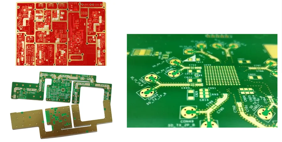
In the world of high-speed communication, radar, and RF systems, the printed circuit board is not just a platform—it’s a signal-critical component. Whether you're building a 24GHz automotive radar, a 77GHz sensor, or a 112 Gbps PAM4 transceiver, your product’s performance depends directly on the integrity of your High Frequency PCB.
At Highleap PCB Factory, we support RF, microwave, and high-speed digital projects across the globe with high frequency PCB manufacturing and assembly services tailored to frequencies ranging from 500 MHz to 80+ GHz. This guide provides a practical overview of how to successfully plan, design, and produce high frequency PCBs—especially when working with China-based high frequency PCB suppliers.
1. Choosing the Right Materials for High Frequency PCB Manufacturing
In High Frequency PCB manufacturing, the material system is one of the most critical choices. Poor laminate selection can lead to insertion loss, skew, impedance drift, or phase instability—especially at GHz ranges.
Common Materials for RF and Microwave Applications
| Material | Dielectric Constant (Dk) | Loss Tangent (Df) | Typical Use Case |
|---|---|---|---|
| Rogers RO4350B | ~3.48 | 0.0037 | General RF/microwave (up to 20 GHz) |
| RO3003 / RO3010 | 3.0–10.2 | 0.0013–0.0022 | Precision RF filters, radar |
| Taconic RF-35 / TLY-5 | 2.2–3.5 | <0.002 | mmWave, phased-array antennas |
| Megtron 6 | ~3.7 | ~0.002 | 28G/56G/112G SERDES and high-speed digital |
| PTFE (Teflon-based) | 2.2 | ~0.0009 | Military, aerospace, ultra-low loss |
At Highleap PCB Factory, we offer stackup modeling and laminate sourcing from Rogers, Taconic, Panasonic, Shengyi, and other qualified suppliers. We help customers find the right balance between electrical performance and manufacturability—especially when looking for cost-effective options in China for high frequency PCBs.
2. Layout and Stackup Best Practices for High-Speed RF PCBs
Layout mistakes in high frequency designs can render a perfect schematic useless. Whether you're targeting 1 GHz or 60 GHz, consistent RF layout is a non-negotiable requirement.
Controlled Impedance and Transmission Line Design
Your trace geometry must support either 50Ω single-ended or 100Ω differential impedance, depending on your application. We routinely work with:
- Microstrip and stripline designs
- Coplanar waveguides with/without ground
- Differential routing with matched length (<5 mils tolerance)
- RF via management (via-in-pad, backdrilling, blind/buried vias)
Layer Stackup Planning
RF boards are rarely standard 4-layer FR4. A typical High Frequency PCB stackup includes:
- Low-Dk core with symmetrical build-up
- Multiple ground/reference planes
- Controlled dielectric thickness between signal layers
- Mixed materials (e.g., PTFE + FR4 outer layers) for cost-effective builds
Before routing, Highleap engineers provide DFM-reviewed stackups with trace width/spacing guidelines that reflect real etch tolerances and plating behavior.
3. How Highleap PCB Factory Enables Fast High Frequency PCB Production
Engineers working on high frequency products often face short design cycles and evolving BOMs. That’s why we’ve developed an RF-friendly workflow focused on speed, precision, and scalability.
Fast High Frequency PCB Manufacturing Capabilities
- Lead time: Prototypes in as fast as 5–7 working days
- Impedance control: ±8% typical (±5% available on request)
- Via options: Laser-drilled microvias, via-in-pad, backdrill
- Material support: Rogers, Taconic, I-Tera, Megtron, and others
- Hybrid stackups: For cost-optimized performance
Whether you're building 5 prototype boards or preparing for 10,000-unit ramp-up, we provide repeatable RF board manufacturing with process transparency.
4. DFM, Assembly and Quality Control in High Frequency PCB Projects
High Frequency PCB assembly is as critical as board fabrication. At high speeds, pad size, solder mask behavior, component placement, and thermal control directly impact SI/PI and radiation.
High Frequency PCB Assembly at Highleap
- RF-specific stencil design to accommodate pad sizes and void control
- X-ray inspection for via-in-pad BGAs or cavity-mounted MMICs
- Low voiding BGA reflow profiles (N2 oven support)
- Precise pick-and-place accuracy for 0201, 01005, or high-Q RF components
- Shield can placement and grounding via fences to reduce EMI
Our turnkey services include full High Frequency PCB assembly, from sourcing matched-value RF components to post-assembly test jigs (SMA, SMP, or coaxial connector fixtures).
5. Why Engineers Choose China-Based High Frequency PCB Suppliers Today
For many global hardware teams, China remains a strategic location for cost-effective and fast High Frequency PCB manufacturing and assembly—but only when the factory has:
- Deep RF/High Speed manufacturing knowledge
- Proven material sourcing network (Rogers, Panasonic, Isola, etc.)
- Engineering support that speaks your design language
- Strong quality documentation (FAI, stackup certs, impedance test reports)
Highleap PCB Factory is based in Shenzhen, China’s technology and electronics hub. We've supported projects across 5G, automotive radar, aerospace, and industrial RF fields. As a dedicated High Frequency PCB factory, we offer:
- Stackup simulations with impedance tuning
- Fast response times (engineering + sales)
- Fluent communication in English, with bilingual CAM teams
- Local material sourcing for lower MOQs and faster builds
- Full production traceability from PCB fab to final assembly
Conclusion: Build High Frequency PCBs With Confidence
Designing and sourcing high frequency PCBs isn't just about signal speed—it’s about engineering discipline, material strategy, and manufacturing capability. Whether you're routing a 77 GHz automotive radar board or assembling a high-speed transceiver module, you need a partner who understands the technical and production realities.
At Highleap PCB Factory, we offer:
- End-to-end High Frequency PCB manufacturing and assembly
- Fast RF prototype turnaround with global shipping
- China-based supply chain advantages with quality-first execution
- Engineering support from stackup design to final inspection
📩 Contact us for your next High Frequency PCB quote—we’ll help you build it right, and build it fast.