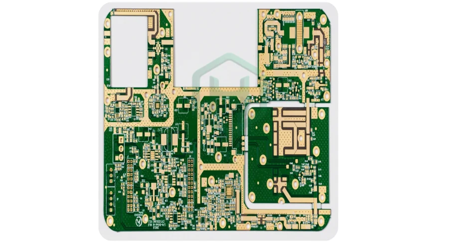
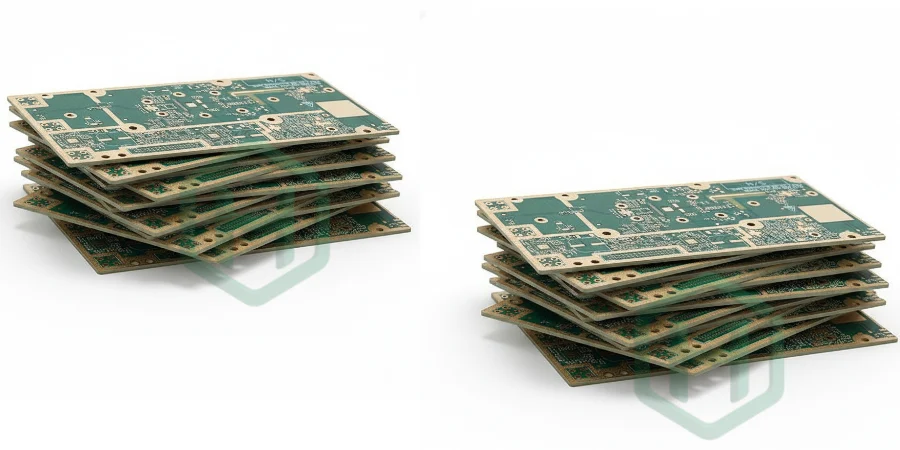
If you are searching for a high-frequency PTFE PCB manufacturer or seeking to understand why PTFE is the essential material for low-loss, high-performance systems, this guide is your definitive resource. The success of today's 5G communications, automotive radar, satellite payloads, and aerospace electronics hinges on the performance of the underlying circuit board. Choosing the right material, mastering the design constraints, and partnering with a capable manufacturer is the difference between a product that underperforms and one that exceeds every expectation.
In this comprehensive guide, we will explore:
- The performance ceiling of FR-4 at high frequencies
- How to select the optimal PTFE laminate for your application
- Actionable design-for-manufacturability (DFM) rules
- The specialized manufacturing processes unique to PTFE
- How performance is verified through testing and quality assurance
- A checklist for selecting a reliable manufacturing partner
- Common applications and frequently asked questions
The Performance Ceiling of FR-4: Why it Fails at High Frequencies
While FR-4 is the workhorse of the PCB industry, it hits a performance ceiling as frequencies rise above 1-2 GHz. It becomes unsuitable for high-frequency applications for two primary reasons:
- High Dielectric Loss: FR-4's epoxy resin system has a high Dissipation Factor (Df), causing it to absorb a significant portion of the signal's energy and convert it to heat. This attenuates the signal and corrupts data.
- High Conductor Loss: The rough copper profile used on standard FR-4, combined with the high-frequency skin effect, dramatically increases resistive losses, further weakening the signal.
In contrast, PTFE laminates are engineered from the ground up for superior signal integrity, making them the default choice for RF and microwave PCBs.
Selecting the Right PTFE PCB Material: A Practical Guide
"PTFE" is not a single material but a family of laminates. Choosing the right one is a critical engineering decision that balances performance, cost, and manufacturability.
| Material Type | Key Advantages | Key Disadvantages | Typical Df (@10 GHz) | Best For... |
|---|---|---|---|---|
| Woven-Glass PTFE | Excellent balance of electrical performance, mechanical stability, and cost-effectiveness. | The glass weave can cause microscopic variations in Dk (fiber weave effect). | 0.001 - 0.002 | General RF/Microwave applications from 1-20 GHz (amplifiers, filters, antennas). |
| Ceramic-Filled PTFE | Extremely low Df, highly stable and isotropic Dk, and improved thermal conductivity. | Highest cost, abrasive nature requires specialized machining and tools. | 0.001 - 0.0015 | Mission-critical mmWave, automotive radar, and satellite communications. |
| Pure PTFE (Unreinforced) | The absolute lowest dielectric constant available, providing maximum signal speed. | Very soft, dimensionally unstable, making multilayer fabrication extremely challenging. | <0.001 | Highly specialized circuits like precision delay lines or unique antenna elements. |
Practical Material Selection Tips
- For 5G mmWave Antennas: Choose ceramic-filled PTFE for its exceptional Dk stability and ultra-low loss.
- For High-Power RF Amplifiers: Woven-glass PTFE provides the necessary mechanical strength and thermal handling capabilities.
DFM: Engineering for Manufacturing Success in High-Frequency PTFE PCBs
A successful high-frequency design must be manufacturable. Follow these critical DFM guidelines:
- Master Your Impedance Model: Use a 2D/3D field solver. Share the specific material datasheet and copper profile (e.g., VLP, RTF) with your manufacturer to ensure their model matches yours.
- Specify Low-Profile Copper: For any application operating above 10 GHz, VLP (Very-Low-Profile) or RTF (Reverse-Treated Foil) copper is a non-negotiable requirement to minimize conductor loss.
- Engineer a Flawless Return Path: Ensure a solid, continuous ground plane under all RF traces. Use liberal via stitching to suppress EMI and prevent unwanted resonance.
- Plan Hybrid Stack-ups Carefully: Combining PTFE with FR-4 can save costs, but you must partner with a manufacturer experienced in bonding dissimilar materials to prevent delamination and reliability issues.

Inside the Factory: The Specialized PTFE Manufacturing Process
Fabricating PTFE PCBs is a science that requires specialized equipment and deep process knowledge.
- Surface Preparation: PTFE's non-stick surface must be chemically altered. We use a plasma activation process or a sodium-based etch to create a receptive surface at a molecular level, ensuring a powerful, reliable bond with copper.
- Precision Drilling: Specialized drill bits and tightly controlled feed/speed rates are used to prevent smearing and deformation of the soft PTFE material, ensuring a pristine hole wall for plating.
- Controlled Lamination: Multilayer PTFE boards are laminated in a vacuum press with precise temperature profiles and low pressure to create a void-free, mechanically stable structure.
- Performance Verification: We use a TDR (Time-Domain Reflectometer) for impedance verification on every panel and a VNA (Vector Network Analyzer) to measure insertion and return loss, providing hard data that the board performs as designed.
How to Select a Capable PTFE PCB Manufacturer
When evaluating a potential high-frequency PTFE PCB supplier, demand evidence of their expertise. Here is a checklist of key qualities:
- Proven Experience: Ask for examples of similar low-loss, high-frequency boards they have fabricated.
- Material Transparency: They should be able to provide full material datasheets and traceability reports.
- Advanced Capabilities: Confirm their ability to handle complex multilayer and hybrid stack-ups.
- In-House Testing: Ensure they have and use VNA/TDR testing equipment for performance verification.
- Engineering Support: A great partner will offer a thorough DFM review of your design before production begins to identify and prevent potential issues.
Applications of High-Frequency PTFE PCBs
This technology is the enabling force behind today's most advanced electronic systems:
- 5G and mmWave Communications - Base stations, phased-array antennas, and transceivers.
- Radar and Automotive Sensing - 77 GHz ADAS systems and beyond.
- Satellite and Aerospace Electronics - High-reliability communication payloads and sensor arrays.
- Test and Measurement Instruments - The core of precision RF/microwave test equipment.
Frequently Asked Questions (FAQs)
Q1: Why is PTFE preferred over FR-4 for RF PCBs? A1: PTFE has an ultra-low dielectric loss (Df) and a stable dielectric constant (Dk) across frequency, which preserves signal strength and integrity. FR-4's losses are too high for reliable RF performance.
Q2: Can PTFE PCBs be multilayer? A2: Yes, absolutely. However, it requires a manufacturer with specialized lamination presses and deep process control expertise to manage the material's soft nature and thermal properties.
Q3: How much does a high-frequency PTFE PCB cost? A3: The cost is significantly higher than FR-4 and varies based on the specific PTFE material, layer count, and design complexity. Ceramic-filled PTFE is the most expensive but offers the highest performance.
Q4: What is the most important question to ask a potential PTFE PCB manufacturer? A4: "Can you show me a TDR report and a VNA plot (S21/S11) from a recent production board that used a similar material to my design?" Their ability to provide and explain this data is a strong indicator of their capability.
Conclusion
A high-frequency PTFE PCB is more than just a component-it is the foundational element that dictates the performance of your entire RF or microwave system. By deeply understanding the materials, adhering to rigorous design principles, and selecting a manufacturing partner with proven expertise, you can ensure your project achieves uncompromising signal integrity, exceptional reliability, and long-term success.

