When modern electronics demand smaller footprints and higher performance, Microvia PCB technology becomes essential. As a leading PCB manufacturer specializing in advanced microvia fabrication, we understand the critical role these precision-engineered boards play in today's most demanding applications—from smartphones and medical devices to automotive electronics and 5G infrastructure.
Our state-of-the-art manufacturing facility combines cutting-edge laser drilling technology with decades of PCB expertise to deliver reliable, high-quality microvia PCBs that meet the strictest industry standards. Whether you need prototype development or high-volume production, we provide comprehensive manufacturing solutions tailored to your specific requirements.
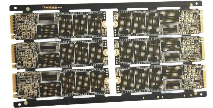
Understanding Microvia Technology: The Foundation of Modern HDI PCBs
Microvia technology represents a significant advancement in printed circuit board manufacturing. These precisely engineered vias, with depths of 0.25mm or less, enable connections between adjacent layers in multilayer PCBs. Unlike traditional through-hole technology, our laser-drilled microvias achieve diameters as small as 75µm, opening new possibilities for compact, high-performance electronic designs.
Our manufacturing capabilities include all major microvia configurations to meet diverse design requirements. Blind vias connect outer layers to inner layers, while buried vias create connections entirely within the PCB stack without affecting surface layers. For complex applications, we produce stacked microvias that align vertically across multiple layers, as well as staggered configurations that provide enhanced structural integrity.
The advantages of our microvia PCBs extend far beyond simple size reduction. These advanced boards deliver superior electrical performance through reduced parasitic effects, enabling faster signal speeds and improved signal integrity. For designers working with fine-pitch components like ball grid arrays (BGAs) and chip-scale packages (CSPs), our microvia technology provides the routing density necessary for successful implementation.
Our quality-controlled manufacturing process ensures each microvia meets stringent specifications for aspect ratio, positional accuracy, and copper plating uniformity. This attention to detail results in reliable interconnections that perform consistently across temperature cycling, mechanical stress, and long-term operation.
Expert Design Support and Manufacturing Capabilities
Successful microvia PCB implementation requires careful coordination between design requirements and manufacturing capabilities. Our experienced engineering team works closely with customers to optimize designs for both performance and manufacturability, ensuring your boards meet electrical specifications while maintaining cost-effectiveness.
We specialize in complex HDI stackup configurations that maximize routing density while maintaining signal integrity. Our most popular configurations include 1+N+1 stackups commonly used in consumer electronics, 2+N+2 designs for higher-density applications, and 3+N+3 configurations for the most demanding high-speed designs. Each stackup is carefully engineered with balanced copper distribution and controlled dielectric properties to minimize warpage and ensure consistent electrical performance.
Our design guidelines emphasize reliability through proven practices developed over years of manufacturing experience. We maintain optimal aspect ratios to ensure reliable via formation and copper plating, specify appropriate annular rings to prevent breakout during drilling, and implement staggered via patterns where beneficial for mechanical strength. For applications requiring via-in-pad technology, we provide copper-filled and planarized solutions that enable direct component mounting without compromising electrical or mechanical integrity.
Signal integrity optimization forms a core part of our design support services. We work with customers to implement proper impedance control, differential pair routing, and reference plane management. Our expertise extends to high-frequency applications where microvia placement and stack symmetry significantly impact performance.
Manufacturing Specifications:
- Via diameters: 75µm to 150µm
- Aspect ratios: Up to 1:1 for optimal reliability
- Layer counts: 4 to 20+ layers
- Minimum trace width: 75µm (3 mil)
- Positional accuracy: ±25µm
- Copper thickness: 0.5oz to 2oz per layer
Advanced Manufacturing Process and Quality Assurance
Our microvia PCB manufacturing process represents the culmination of advanced technology and rigorous quality control. Every board undergoes precision laser drilling using state-of-the-art CO₂ and UV laser systems that deliver clean, accurate holes without thermal damage to surrounding materials.
The manufacturing sequence begins with careful material preparation and stack planning. Each layer undergoes thorough inspection before processing, ensuring optimal material properties and dimensional stability. Our laser drilling process utilizes computer-controlled systems with automatic vision alignment, achieving positional accuracies within ±25µm across the entire panel.
Following drilling, our plasma desmearing process removes resin residue and prepares via walls for reliable copper adhesion. This critical step ensures consistent plating quality and long-term reliability. Our electroless copper deposition creates a uniform seed layer, followed by electrolytic copper plating that builds wall thickness to specification.
For applications requiring enhanced reliability, we provide copper-filled microvias using specialized plating techniques that eliminate voids and ensure consistent electrical performance. Our via capping process creates planar surfaces suitable for component mounting and solder mask application.
Quality Control Measures:
- Automated optical inspection (AOI) at each process step
- X-ray imaging for void detection and fill quality verification
- Microsectioning analysis for wall thickness and adhesion verification
- Electrical testing including continuity, isolation, and impedance
- IPC-6012E and IPC-2226 compliance verification
- ISO 9001:2015 and ISO 13485 certified processes
Our quality management system ensures consistent results through statistical process control, comprehensive documentation, and continuous improvement initiatives. Each production lot undergoes thorough testing and inspection before shipment, providing customers with reliable, specification-compliant products.
Industry Applications and Custom Solutions
Our microvia PCB manufacturing serves diverse industries where performance, reliability, and miniaturization are paramount. In consumer electronics, we produce boards for smartphones, tablets, wearables, and gaming devices where space constraints demand maximum routing density. Our automotive-grade manufacturing supports automotive electronics including advanced driver assistance systems (ADAS), radar modules, and electric vehicle power management systems.
The medical device industry relies on our precision manufacturing for implantable devices, diagnostic equipment, and portable monitoring systems. Our ISO 13485 certification and biocompatible material options ensure compliance with stringent medical device regulations. For telecommunications and networking applications, we manufacture high-frequency boards for 5G infrastructure, base stations, and high-speed networking equipment.
Aerospace and defense customers benefit from our capability to produce boards meeting military specifications and space-qualified standards. We maintain appropriate security clearances and follow ITAR compliance protocols for sensitive applications.
Beyond standard applications, we excel at custom solutions for unique requirements. Our engineering team collaborates with customers to develop specialized stackups, material combinations, and processing techniques that meet specific performance criteria. Whether you need boards for harsh environments, extreme temperatures, or unusual form factors, we have the expertise and flexibility to deliver effective solutions.
Application Examples:
- Smartphone main boards and RF modules
- Automotive radar and camera systems
- Medical implants and diagnostic sensors
- 5G base station RF boards
- Satellite communication systems
- High-speed computing and AI accelerators
- IoT sensors and wearable devices
- Industrial automation controllers
Partnership Approach and Manufacturing Excellence
Choosing the right PCB manufacturer involves more than evaluating technical capabilities. We believe in building long-term partnerships through responsive communication, flexible manufacturing approaches, and consistent delivery performance. Our customer service team works closely with your engineering and procurement teams to ensure smooth project execution from initial design review through final delivery.
Our manufacturing flexibility accommodates both prototype development and high-volume production requirements. For rapid prototyping, we offer expedited services with turnaround times as short as 5-7 days for standard configurations. Our volume production capabilities scale efficiently to support your market demands while maintaining consistent quality and competitive pricing.
Global logistics support ensures reliable delivery regardless of your location. We maintain strategic shipping partnerships and inventory management systems that minimize lead times and shipping costs. Our packaging and handling procedures protect boards during transit while supporting your just-in-time manufacturing requirements.
Manufacturing Capabilities Summary:
- Daily production capacity: 10,000+ square meters
- Prototype turnaround: 5-7 days typical
- Volume production scaling: 100 to 100,000+ pieces
- Global shipping with tracking and insurance
- Technical support in multiple languages
- Design for manufacturing (DFM) analysis
- Cost optimization consulting
- Supplier quality audits and certifications
Our commitment to continuous improvement drives ongoing investments in equipment, training, and process optimization. We regularly evaluate new technologies and manufacturing techniques to maintain our position at the forefront of microvia PCB manufacturing excellence.
Ready to Start Your Next Project?
Partner with our experienced team for reliable microvia PCB manufacturing that meets your performance, quality, and delivery requirements. Contact us today to discuss your specific needs and receive a detailed quotation for your project.