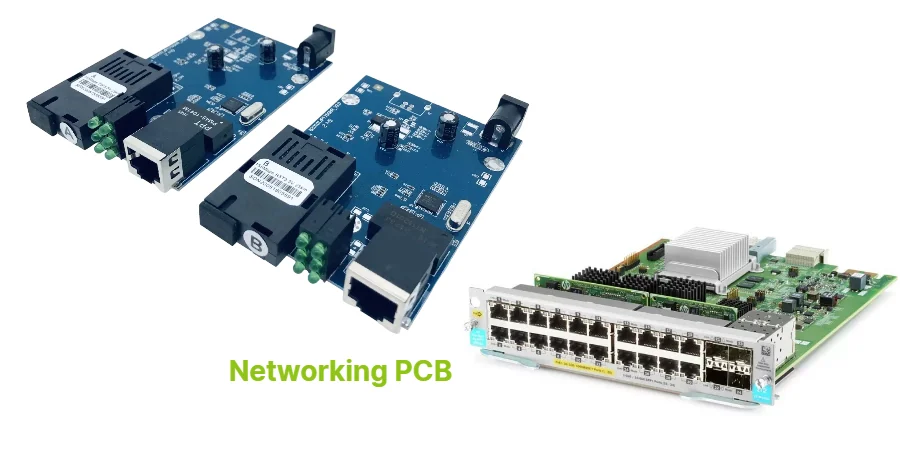
Networking PCBs form the backbone of our connected world—from enterprise routers and switches to telecom infrastructure and IoT gateways. Highleap PCB Factory (HILPCB) specializes in manufacturing and assembling these complex boards with a focus on impedance control, EMI management, and reliable signal transmission. Our expertise helps engineers tackle challenges in high-speed digital interfaces, RF coexistence, power distribution, and thermal management.
Networking PCB Requirements and Routing Priorities
Modern networking hardware demands precision in layout and material selection to maintain signal integrity and electromagnetic compatibility:
High-speed interfaces: Equipment supporting 1G–400G Ethernet, SerDes fabrics, and backplane connections requires meticulous length/phase matching, controlled impedance, and careful via stub management. Our high-frequency PCB capabilities ensure reliable multi-Gbps channels.
RF and wireless sections: Wi-Fi, 5G, LTE, and other wireless technologies demand special attention to microstrip/stripline design and material selection. Our Rogers PCB manufacturing supports antennas, filters, and sensitive RF front-ends.
Multilayer architectures: Typical networking boards utilize 8–20+ layers with dedicated ground planes and strategic via stitching to maintain signal integrity and manage EMI.
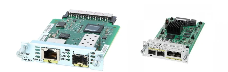
Networking peripherals: Complete solutions often include daughter cards, SFP/QSFP cage breakouts, POE power distribution boards, and management modules for flexible product configurations.
Critical design practice: Always maintain continuous reference planes under high-speed pairs, avoid ground plane splits in signal paths, and implement via fences at layer transitions to control EMI.
Materials and Stackup Selection for Networking Hardware
Networking PCB material selection requires balancing performance requirements against cost constraints in ways that optimize the final product. Most designs benefit from a hybrid approach, starting with high-Tg FR-4 as the foundation for control planes and lower-speed interfaces. This material offers excellent thermal stability, mechanical strength, and reasonable signal performance at an economical price point. The question of whether premium laminates are necessary depends primarily on signal loss budgets and frequency requirements. For 10G-100G Ethernet channels or sensitive RF sections, selective incorporation of low-loss laminates like Rogers materials dramatically improves insertion loss characteristics and signal quality while keeping overall board costs manageable.
Advanced HDI structures play a crucial role in modern networking equipment, particularly around dense BGA components and connector arrays. Implementing skip/stacked microvias in these congested areas reduces signal stubs, minimizes layer transitions, and creates cleaner routing channels that improve both signal integrity and manufacturing yields. Surface finish selection significantly impacts long-term reliability, with ENIG or immersion silver providing the optimal combination of planarity for fine-pitch components and corrosion resistance for high-cycle connector interfaces that must maintain consistent contact resistance over years of operation in varying environments.
EMC management represents a particular challenge for networking PCBs that combine high-speed digital circuits with wireless capabilities. Effective strategies include implementing guard traces and stitching vias around noisy power conversion sections, establishing clean chassis bonding points that avoid creating ground loops, and carefully isolating shield structures from signal return paths except at designated connection points. This integrated approach to material selection, stackup design, and EMC planning ensures networking equipment meets both performance and regulatory requirements. Our online impedance calculator helps designers align trace geometries with specific material parameters for precise impedance control across all critical transmission lines.
Assembly, Test, and Field Reliability
Networking equipment often operates continuously for years in various environments, requiring robust assembly and comprehensive testing:
Advanced assembly: We handle fine-pitch ASICs, specialized RF modules, and shield cans with controlled reflow profiles and strict coplanarity verification through our sophisticated assembly facilities.
Comprehensive inspection: AOI and X-ray inspection of hidden joints ensure assembly quality before functional testing.
Functional validation: We support link establishment testing (1G/10G/100G), bit error rate testing on sample ports, POE load testing, and thermal profiling under specified airflow conditions.
Documentation: All builds include detailed material certifications, test logs, and lot traceability for quality assurance and regulatory compliance.
Reliability enhancement: Consider specifying conformal coating for high-humidity installations, verify SFP/QSFP cage solder wick control, and implement proper ESD discharge paths to chassis ground points.
Cost, Lead Time, and Sourcing Essentials
Understanding key cost drivers and planning accordingly improves both performance and budget outcomes:
Major cost factors: Layer count, percentage of low-loss materials, HDI via structures, connector/cage density, and specialized RF sections requiring premium laminates.
Typical lead times: Prototypes 7–12 business days; production runs 2–4 weeks depending on stackup complexity and test requirements.
Documentation checklist: Comprehensive fabrication notes, impedance tables, finish specifications, back-drill maps (if applicable), RF keepout zones, chassis bonding points, and a detailed test matrix.
Before finalizing designs, use our Gerber viewer for pre-release verification and collaborate with our engineering team on stackup and material selection to prevent costly revisions.
Why HILPCB for Networking PCB Projects
High-speed and RF expertise: Proven experience with Ethernet fabrics up to 400G, RF coexistence layouts, and optimized material combinations that control costs without sacrificing performance.
Manufacturing discipline: Strategic use of HDI where it delivers value, with conservative tolerances elsewhere to maximize production yield and reliability.
Comprehensive testing: Complete support for bring-up validation, BER testing on sample lanes, and thermal/POE characterization for field-ready confidence.
Frequently Asked Questions
Do I always need Rogers/PTFE materials for Networking PCBs?
No—many designs effectively use high-Tg FR-4 for digital sections and reserve Rogers PCB or other low-loss materials only for RF portions or exceptionally long high-speed links.How do you ensure signal integrity across dense connector arrays and ASICs?
We establish stackup parameters early, implement HDI fan-out via HDI PCB where needed, apply back-drilling for stub reduction, and verify geometry using our impedance calculator.Can you assemble high-density boards with RF shields and fine-pitch BGAs?
Yes—our advanced assembly processes handle fine-pitch components and shielded sections with comprehensive AOI, X-ray inspection, and functional testing.What are typical prototype and production timelines?
Prototypes typically require 7–12 business days; production runs average 2–4 weeks depending on layer count, HDI requirements, and test specifications.How do you address EMC and ESD concerns?
We review plane continuity, via fence implementation, guard traces, shield bonding strategy, and chassis grounding points during the DFM phase to prevent EMC/ESD issues before production.Do you manufacture networking PCB peripheral products?
Yes—we regularly produce daughter cards, POE power modules, interface boards, and management PCBs as part of comprehensive networking solutions.What documentation should I provide for efficient manufacturing?
Include detailed impedance tables, finish specifications, stackup requirements, back-drill parameters, connector footprints with associated keepouts, RF zones, and functional test requirements. Use our Gerber viewer before final submission to identify potential manufacturing issues.