Why Choosing the Right PCB Design Tool Matters
Designing a printed circuit board (PCB) is a complex task that involves electrical, mechanical, manufacturing and testing aspects. The software you use has a direct impact on:
- how efficiently you convert schematics into board layouts,
- how reliably you meet manufacturing constraints (like trace widths, clearances, via types, stack-up definitions),
- how smoothly you collaborate across disciplines (mechanical, electrical, manufacturing), and
- how readily you prepare the board for fabrication and assembly.
A good PCB design tool helps avoid costly redesigns, shortens development time, improves yield in manufacturing, and ensures the final product is robust.
Leading PCB Design Tools and What They Offer
Here are some of the most widely used PCB design solutions today:
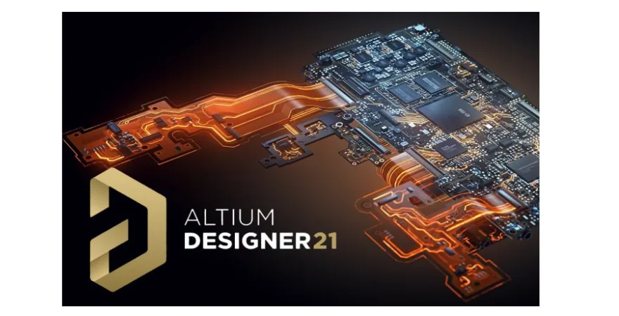
Altium Designer
A premium all-in-one tool for professional PCB design. It provides schematic capture, advanced layout, 3D visualization, MCAD integration, extensive library and simulation support. It is ideal for high-speed, multi-layer, high-complexity boards.
Best for: enterprise teams, demanding designs
Considerations: higher cost, steeper learning curve
KiCad
An open-source, free tool that has grown significantly in capability. It offers schematic capture, PCB layout, 3D viewing, and manufacturing file output. Great for hobbyists, education, startups and cost-sensitive projects.
Best for: small teams, prototypes, low-budget production
Considerations: fewer advanced features than high-end tools
Autodesk EAGLE
A mid-range tool popular among makers, startups and small teams. It provides schematic and layout functionality, component libraries and cloud-based services. Good balance of cost and features.
Best for: smaller projects, embedded development
Considerations: less suited for very large, high-speed or multi-layer enterprise designs
OrCAD
A professional tool with strength in schematic capture and simulation, layout integrated. Suitable for moderate complexity boards.
Best for: engineers working in commercial environments needing simulation plus PCB layout
Considerations: cost and feature set still below top-tier routing/simulation packages
Cadence Allegro
A high-end solution used in very large, complex projects (automotive, telecom, aerospace). Supports advanced routing, differential pairs, power integrity, multi-channel systems.
Best for: high-budget, high-complexity, mission-critical projects
Considerations: very high cost, significant training required
Key Features to Evaluate When Selecting PCB Design Tools
When comparing different tools, you should examine the following critical features:
Schematic Capture & Netlist Generation
How easily can the software turn your circuit diagram into a formal netlist for layout? Does it support hierarchical designs, symbol libraries and connectivity checks?
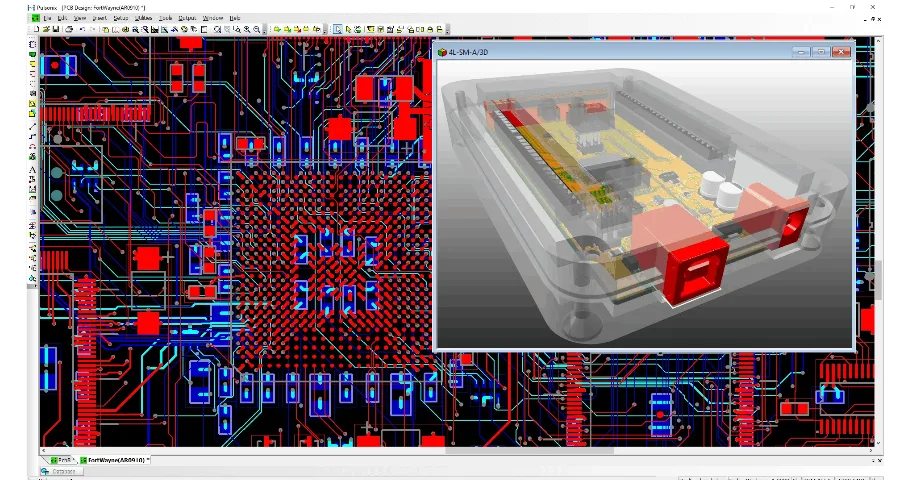
PCB Layout & Routing Engines
Look for robust routing functionality (manual + auto), support for differential pairs, impedance control, multilayer routing, via types (through-hole, blind, buried, micro-via).
Design Rule Checking (DRC) & Design for Manufacturability (DFM)
Strong DRC capability ensures your design meets manufacturing constraints (clearances, trace widths, via sizes). DFM support helps validate the output before sending for fabrication.
3D Visualization & Mechanical Integration
Board layouts today must often integrate with mechanical enclosures. A tool with 3D visualization and MCAD integration helps reduce mismatch between board and housing.
Library/Footprint Management
Accurate and up-to-date component libraries (symbols, footprints, 3D models) speed design and reduce manufacturing errors. Ability to manage custom libraries is a plus.
Simulation & Signal/Power Integrity
For high-speed, mixed-signal or dense designs, simulation capabilities (SI/PI/thermal) help catch issues early rather than in costly prototypes.
Manufacturing Output Support
Ensure the tool can export all necessary manufacturing files: Gerbers, drill files, pick & place data, BOM, ODB++/IPC-2581. Compatibility with fabricators is vital.
Collaboration & Version Control
Multi-user environments benefit from cloud collaboration, version control, revision history, access control. Useful for teams spread geographically.
Cost & Licensing Model
Tools vary widely in cost (free/open source, perpetual license, subscription). Consider total cost of ownership, training, support and scalability.
Typical PCB Design Workflow
Here is a high-level workflow you’ll encounter when designing PCBs with proper tools:
- Define design requirements: materials, layer count, copper weight, impedance, size, cost.
- Schematic capture: draw the circuit, place components logically, define nets and power rails.
- Set up design constraints: trace widths, clearances, via types, keep-out zones, high-speed nets.
- Component placement: position components on the board considering signal flow, thermal, assembly and manufacturing.
- Routing and via planning: route signals, differential pairs, ensure impedance and via strategy are correct.
- 3D/Mechanical check: ensure board fits the enclosure, check mechanical collisions and mounting.
- DRC/DFM verification: run rule checks and manufacturing readiness checks before export.
- Generate manufacturing outputs: production files such as Gerbers, drill files, BOM, pick/place, panelization.
- Prototype and testing: fabricate prototype boards, test functionality, performance, thermal behavior.
- Production: finalize design, hand off to manufacturer, assembly and testing.
- Revision and lifecycle support: manage updates, documentation, spare parts and version control.
Avoiding Common Pitfalls
- Selecting a tool based purely on budget and then discovering it lacks needed advanced features.
- Ignoring the quality of component libraries; inaccurate footprints cause board issues.
- Skipping mechanical/3D integration, leading to enclosure fit failures.
- Not validating manufacturing readiness (DFM) causing delays or scrap.
- Underestimating training needs and ramp time for complex tools.
Conclusion
Choosing the right PCB design tool is essential for the success of your project, as it influences every stage from design to manufacturing. For simple projects, affordable tools like KiCad or Autodesk EAGLE may suffice, but for complex, high-speed, or multi-layer designs, more advanced tools like Altium Designer or Cadence Allegro are necessary. These advanced tools offer features such as high-precision routing, signal integrity checks, and 3D visualization, ensuring that the design meets performance, electrical, and mechanical requirements.
The right PCB design tool also ensures smooth integration with the manufacturing process. It helps generate the required production files-such as Gerbers, drill files, and BOMs-while incorporating Design for Manufacturability (DFM) and Design Rule Checking (DRC) to prevent production issues. By selecting the appropriate software, you can streamline the design process, reduce errors, improve product quality, and ensure efficient, cost-effective manufacturing.
FAQ
Q1: Can I switch PCB design tool mid-project?
A1: Technically yes, but migrating existing schematics, layouts and libraries can be time-consuming and risky. Planning ahead is strongly recommended.
Q2: Is open-source software like KiCad sufficient for commercial production?
A2: Yes-many commercial boards are produced with open-source tools. The key is ensuring your libraries, constraints and output files are production-ready.
Q3: How do I know if a design tool outputs files compatible with my board manufacturer?
A3: Verify the manufacturer’s preferred file formats and process capabilities (layer count, copper weight, via types), then check the tool can produce those outputs correctly.
Q4: What features justify investing in high-end tools rather than simpler ones?
A4: If your board involves many layers, high-speed signals, strict impedance control, or you need integrated simulation and team workflows, high-end tools pay off. Simpler designs may use lower-cost tools.
Q5: How important is library management in PCB design tools?
A5: Very important. Accurate symbols, footprints and 3D models help avoid assembly errors, manufacturing delays and rework, which may cost far more than the tool itself.