Field failures cost 10-50× more than catching defects during manufacturing. A single failure destroys customer confidence, generates warranty returns, and damages reputation. But over-testing wastes time and money on unnecessary procedures. The right test strategy balances thoroughness with cost-effectiveness based on your specific needs.
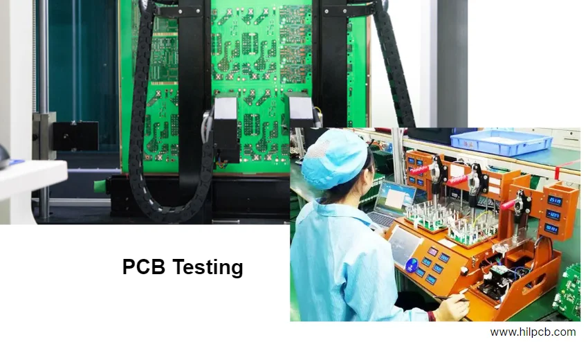
HILPCB provides complete testing services from prototype validation through volume production quality assurance. Our testing recommendations match your production volume, board complexity, and quality requirements.
Flying Probe vs In-Circuit Testing: Which One You Actually Need
The "best" electrical test method depends entirely on your production volume. Choose wrong and you either waste money on unnecessary fixtures or create production bottlenecks with slow test times.
Flying Probe Testing - The Prototype and Low Volume Choice
Movable probes contact test points under software control, checking connectivity and component presence without custom fixtures. Perfect for prototype quantities and low volume production where ICT fixture costs cannot be justified.
Key advantages:
- Zero fixture cost - test program created from Gerber files in 2-4 hours
- Design changes accommodated instantly with simple program updates
- Typical test time: 3-8 minutes per board depending on complexity
- Ideal volume range: 5-500 boards total
Limitations to understand:
- Slow test times create bottlenecks in volume production
- Cannot power circuits to test active components - only checks passive values and connectivity
- Limited access on dense boards where test points are blocked by components
Cost breakeven typically occurs around 500-1000 boards total. Below this quantity, flying probe wins. Above this quantity, ICT fixture investment pays back through faster test times.
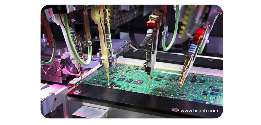
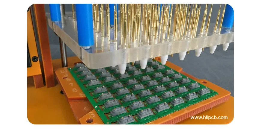
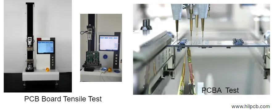
In-Circuit Testing (ICT) - The Volume Production Standard
Bed-of-nails fixture with fixed probe positions contacts multiple test points simultaneously, completing full board test in 30-90 seconds. Requires custom fixture costing $50-$15,00 depending on board size and pin count.
Why volume production uses ICT:
- Tests complete boards in 30-90 seconds versus 3-8 minutes for flying probe
- Powers up board and tests individual component values
- Verifies correct component placement and orientation
- Checks for solder bridges and opens
- Diagnostic capability pinpoints specific failed components
The fixture investment hurdle:
- Initial cost: $50-$15,00 per board design
- Program development: 1-2 weeks including fixture design and debug
- Design changes require fixture modification: $100-$3,000 and 1-2 week delay
- Board design must provide test point access to critical nets
Volume production of 1,000+ boards annually justifies ICT investment. Our PCB assembly production lines use ICT as standard for all volume contracts exceeding 500 boards per year.
Visual Inspection Methods: When Automation Helps and When It Doesn't
Visual inspection catches different defect types than electrical testing. The question isn't whether to inspect but which inspection methods match your requirements and volume.
Manual Visual Inspection - The Required Baseline
Every board receives manual inspection regardless of automated systems employed. Trained inspectors examine boards under magnification checking for:
- Misaligned components affecting mechanical fit
- Solder bridges shorting adjacent pins
- Missing or wrong components
- Damaged boards or components
- Contamination that affects reliability
Manual inspection speed: 2-5 minutes per board. Consistency issues emerge during long production runs as inspector fatigue sets in. Cannot see hidden joints under BGA packages or inside connectors.
Works as primary method for prototype quantities under 100 boards. Requires supplement with automated methods for volume production to maintain consistency.
Automated Optical Inspection (AOI) - Production Efficiency
High-resolution cameras capture images and compare against reference database or golden board template. Inspection completes in 30-90 seconds per board, enabling integration into high-volume production lines.
AOI catches 95%+ of solder defects:
- Insufficient solder or excess solder volume
- Solder bridges between adjacent pins
- Solder balls on board surface
- Tombstoning (component standing on end)
- Component shifting during reflow
Component placement errors get flagged automatically:
- Wrong parts installed
- Missing components
- Rotated polarized components (diodes, electrolytic capacitors, ICs)
- Misalignment exceeding tolerances
Limitations to understand:
- Cannot inspect hidden joints under BGA packages or inside connectors
- Programming requires 2-4 hours per new board design for template development
- False positives slow production when AOI flags acceptable boards as defective
Our production lines use post-reflow AOI on all orders exceeding 100 boards. Catches most assembly defects while components can still be reworked easily. Pre-reflow solder paste inspection (SPI) prevents problems by catching paste deposition errors before component placement.
X-Ray Inspection - Required for BGA and Hidden Joints
X-rays penetrate component bodies to image solder joints beneath BGA packages, QFN thermal pads, and other hidden connections. Only method to verify these critical joints without destructive testing.
What X-ray inspection reveals:
- Void percentage in solder joints (critical for thermal and mechanical reliability)
- Bridging between adjacent balls invisible to optical inspection
- Insufficient solder or missing balls
- Package alignment and centering on pads
Every BGA component requires X-ray inspection per IPC standards for Class 2 and Class 3 products. Our PCB manufacturing process includes X-ray of all BGA, QFN, and bottom-terminated components with detailed reports provided.
Functional Testing Strategies
Electrical and visual testing verify assembly quality but don't confirm the product actually works. Functional testing validates end-to-end system operation under real conditions.
When Functional Testing Becomes Necessary
Simple boards with few active components might not need functional testing - electrical testing suffices. Complex assemblies with processors, memory, and multiple interfaces require functional validation to catch:
- Firmware loading and execution issues
- Communication interface functionality
- Sensor calibration and response
- Power sequencing and management
- System-level interactions electrical testing cannot verify
Functional Test Development Process
Test fixture design accommodates board-specific connectors and interfaces. Test procedure development defines:
- Power-on sequence and timing
- Interface exercising (USB, Ethernet, serial, etc.)
- Pass/fail criteria for each functional element
- Test time targets for production throughput
- Data logging and traceability requirements
Test development typically requires 2-4 weeks including fixture fabrication, software development, and procedure validation. Initial investment of $3,00-$10,00 depending on complexity, justified for production volumes exceeding 500 boards annually.
Boundary Scan (JTAG) Testing
Complex digital designs with processors and FPGAs often include JTAG boundary scan capability. Enables testing of complex chips without physical access to all pins. Requires design-for-test consideration during layout phase.
Boundary scan advantages:
- Tests internal chip functionality without external test points
- Validates interconnections between JTAG-enabled devices
- Programs and verifies flash memory contents
- No custom fixture required beyond JTAG connector access
Works as supplement to other test methods, not complete replacement. Best for high-density digital designs where traditional test access is limited.
Test Strategy Selection Based on Production Volume
Matching test methods to production volume prevents both under-testing and wasteful over-testing. Our recommendations based on thousands of designs:
Prototype Quantities (5-50 boards)
- Manual visual inspection
- Flying probe electrical testing
- Functional testing as needed for validation
Total test cost per board: $15-$35 depending on complexity. No fixture investments required.
Low Volume Production (50-500 boards)
- Manual visual inspection
- Flying probe electrical testing
- Functional testing for complex designs
Test time per board: 5-10 minutes total. Suitable for batches up to 100 boards monthly without creating bottlenecks.
Medium Volume Production (500-5000 boards annually)
- Automated optical inspection (AOI)
- In-circuit testing (ICT) with custom fixture
- Functional testing for complex assemblies
- X-ray inspection for BGA components
Fixture investments of $50-$20,00 total amortize across production volume. Test time reduces to 2-4 minutes per board, enabling higher throughput.
High Volume Production (5000+ boards annually)
- Full automated inspection and testing
- Statistical process control monitoring
- Periodic destructive testing for ongoing validation
- Automated functional testing with custom fixtures
Complete test strategy optimized for throughput and cost. Our PCB assembly lines handle volume production with integrated testing ensuring consistent quality.
Quality Documentation and Traceability
Comprehensive documentation is essential for effective PCB testing, whether for bare boards or assemblies. At HILPCB, every PCB undergoes fully traceable inspection and testing, ensuring electrical reliability and manufacturing consistency.
Each PCB Test Report Includes:
- Electrical continuity and isolation test results with pass/fail details
- Visual and microscopic inspection records showing surface quality and defects corrected
- X-ray images (for multilayer PCBs) verifying via integrity and internal layer alignment
- Functional test data for finished PCBs where applicable
- Material and process lot traceability for laminates, copper foil, and surface finishes
All reports are delivered electronically with every shipment and stored securely for long-term reference, supporting warranty verification and root-cause analysis when needed.
Process Control and Continuous Improvement
In PCB manufacturing, HILPCB employs Statistical Process Control (SPC) to detect deviations before defects occur. Parameters continuously monitored include:
- Inner layer registration and drilling accuracy
- Copper plating thickness and uniformity
- Lamination temperature and pressure curves
- Electrical test yields and recurring failure patterns
Analyzing this data enables ongoing process refinement, higher yields, and more consistent board performance.
From prototype validation through high-volume PCB fabrication, HILPCB’s testing and documentation system ensure measurable quality, full traceability, and long-term reliability for every circuit board delivered.