As power density increases in modern electronic systems, the role of the Power PCB becomes more than just mechanical support—it becomes a critical component in thermal, electrical, and reliability performance. Whether you're designing a 5V buck converter, a 60V motor controller, or a 600W power amplifier, how you design and manufacture the Power PCB directly influences efficiency, noise, safety, and product life.
At Highleap PCB Factory, we support global OEMs and engineers with high-current, high-reliability Power PCB manufacturing and assembly. This guide offers a practical overview of what makes a Power PCB different, how to lay it out properly, and what considerations go into building it right—from material choice to copper thickness to thermal management.
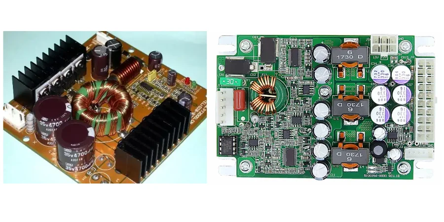
1. What Makes a PCB a “Power PCB”?
A Power PCB is a circuit board designed to carry substantial current—often several amps to tens of amps—without introducing excessive voltage drop, heat buildup, or EMI issues. Compared to signal or logic boards, Power PCBs are engineered with:
- Wide copper traces or copper pours
- Thicker copper layers (e.g., 2 oz to 6 oz)
- Robust thermal vias and planes
- Short, low-inductance current paths
- Heat-sensitive component spacing and clearance rules
Power PCBs are common in:
- Power supply modules (AC-DC, DC-DC)
- LED drivers and lighting control boards
- Motor controllers and drives
- Battery charging circuits and BMS
- Industrial automation equipment
- High-wattage consumer devices (e.g., power tools, e-bikes)
At Highleap, we design and produce custom Power PCBs for both low-voltage (5V–24V) and high-voltage (48V–600V) systems with strict adherence to IPC and creepage standards.
2. Core Design Rules for Power PCB Layout
a. Copper Thickness and Trace Width
One of the defining features of a Power PCB is heavy copper usage. Typical logic PCBs use 1 oz copper, but for power applications, we often recommend 2 oz, 3 oz, or more depending on current load and thermal requirements.
Using IPC-2152 guidelines, trace width must be calculated for both internal and external layers. For example:
- 10A current at 2 oz copper with 10°C rise → ~200 mil trace width
- Internal layers may require even wider routing or parallel paths
We help customers determine appropriate trace width, spacing, and layer count early in the design process to avoid late-stage rework.
b. Minimize Loop Area
Current loops generate unwanted magnetic fields and EMI. A proper power-ground loop should be tight and directly coupled via a solid reference plane. Layout tips include:
- Place input/output capacitors close to switches
- Avoid routing long, exposed power loops
- Route high di/dt signals over continuous planes
c. Thermal Path Engineering
Power PCBs generate heat, and PCB layout must actively manage it. Strategies include:
- Copper pours to spread and sink heat
- Thermal vias under MOSFETs, diodes, and regulators
- Heat islands and copper slugs on the top/bottom layers
- Mounting holes aligned with external heatsinks
Highleap provides thermal simulations and DFM feedback on component placement and via density to optimize heat dissipation.
Before sending your design to production, you can preview the layout using our free online Gerber Viewer to inspect your copper layers, vias, and component placements.
3. Material and Stackup Considerations for Power PCBs
The choice of base material and layer structure is critical in ensuring mechanical and thermal stability of Power PCBs, especially under repeated load cycling or high-temperature conditions.
a. FR4 vs High-Tg Materials
Standard FR4 may work for low-power boards, but for sustained temperatures >130°C or heavy copper layers, we recommend:
- High-Tg FR4 (>170°C Tg)
- Halogen-free laminates for regulatory compliance
- Metal-core PCB (MCPCB) or aluminum-backed substrates for LED and high-density modules
b. Stackup Design
For multi-layer Power PCBs, copper balance across layers is key. Unbalanced stackups lead to warping or delamination during reflow. A well-designed power board might look like:
- L1: Signal and light power (2 oz)
- L2: Solid GND
- L3: Power distribution (3 oz)
- L4: Return plane + auxiliary signals
Highleap helps design symmetrical, thermally optimized stackups for Power PCB manufacturing in China that meet both cost and reliability targets.
4. Power PCB Assembly: Challenges and Process Control
High current boards bring additional risks during assembly. Thick copper causes uneven heating, and large copper areas act as thermal sinks during reflow soldering.
a. Reflow Profile Tuning
For 2 oz+ copper layers, standard reflow profiles may result in cold solder joints. We tune oven profiles to account for:
- Thermal mass
- Component height variation
- Large copper fills under QFNs or DPAKs
We also use step stencils to control paste volume where needed.
b. Wave and Selective Soldering
Power PCBs often contain large through-hole components like terminal blocks, inductors, and transformers. These require:
- Higher solder pot temperature
- Slower conveyor speeds
- Preheat zones to prevent thermal shock
Highleap’s Power PCB assembly lines support both wave soldering and selective soldering, depending on the design.
c. Quality Control
Every Power PCB is inspected using:
- AOI for SMT placement
- X-ray for BGA/QFN solder joints
- Electrical testing (E-test)
- Optional functional testing with load simulation (upon request)
To test switching behavior, voltage drop, or thermal stress in your power designs, try our free online circuit simulator. It’s a great way to validate concepts before prototyping.
5. Why Engineers Choose Highleap for Power PCB Manufacturing in China
Choosing the right Power PCB factory is about more than copper weight. It’s about understanding how current, heat, and material behavior intersect in a real production environment.
At Highleap PCB Factory, we offer:
- Rapid prototype to mid-volume Power PCB production
- Power PCB assembly with both SMT and THT capabilities
- Thermal management expertise from layout to reflow
- China-based pricing with international engineering standards
- Bilingual support team for collaboration across time zones
Our engineers regularly assist customers with fast Power PCB manufacturing projects where deadlines, cost, and reliability all matter. Whether it's a 5-layer 3 oz DC bus or a compact AC-DC converter, we bring the process experience to help you succeed.
Conclusion
Power PCBs are more than just copper—they are the foundation of your product's performance and reliability. As voltage levels rise and space becomes tighter, engineers must think about heat, loop area, trace impedance, and manufacturability from day one.
At Highleap PCB Factory, we’re committed to supporting power electronics engineers with cost-effective, technically sound, and fast-turn Power PCB solutions. Our services span from DFM consultation to full turnkey assembly.
📩 Contact us to request a Power PCB quote or get feedback on your design—we’ll help you bring power to your product, reliably.