In the world of high-frequency electronics, signal integrity is everything. For RF, microwave, and 5G systems where every fraction of a decibel matters, PTFE (Polytetrafluoroethylene) circuit boards are the undisputed cornerstone. At HILPCB, we specialize in manufacturing and assembling high-performance PTFE boards, ensuring consistent impedance, minimal signal attenuation, and precise dimensional stability from prototype to production.
- Why Choose PTFE for High-Frequency Circuits?
- Key Electrical Properties That Define PTFE Performance
- Where Are PTFE Circuit Boards Used? Key RF and Microwave Applications
- Mastering PTFE Fabrication: How We Overcome Key Manufacturing Hurdles
- Critical Design Guidelines for High-Performance PTFE PCBs
- Ensuring Performance: Our Rigorous Testing and Quality Assurance Protocol
Why Choose PTFE for High-Frequency Circuits? {#why-choose-ptfe}
A PTFE circuit board is a printed circuit built on a high-performance fluoropolymer renowned for its exceptional stability at high frequencies. Unlike standard epoxy-based materials like FR-4, PTFE offers an ultra-low and remarkably stable dielectric constant (Dk), typically between 2.0 and 2.6. This stability is maintained across a vast range of frequencies and operating temperatures, which is absolutely essential for preserving signal integrity in sensitive microwave circuits.
To enhance its mechanical properties, PTFE is often reinforced with woven glass or ceramic fillers. This creates a robust substrate that combines the electrical purity of PTFE with the physical durability needed for real-world applications.
Key Electrical Properties That Define PTFE Performance {#electrical-properties}
The superiority of PTFE for high-frequency applications is defined by these critical material properties:
| Property | Typical Range | Significance for Your Circuit |
|---|---|---|
| Dielectric Constant (Dk) | 2.0 - 2.6 | A low and stable Dk enables faster signal propagation and makes achieving precise impedance control easier. |
| Dissipation Factor (Df) | 0.0009 - 0.002 | This ultra-low value signifies minimal signal energy lost as heat, ensuring maximum signal power reaches its destination. |
| Thermal Conductivity | 0.25 - 0.6 W/m·K | Helps dissipate heat from active components, improving system reliability. |
| Moisture Absorption | <0.02% | Virtually immune to humidity, ensuring dielectric properties remain stable in any environment. |
| Z-axis CTE | 120-250 ppm/°C | Controlled with fillers to enhance the long-term reliability of plated through-holes (vias). |
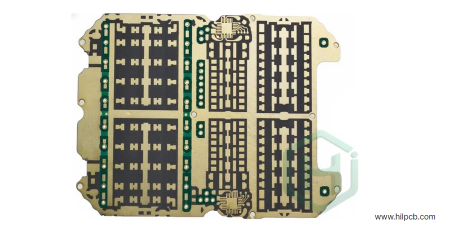
Where Are PTFE Circuit Boards Used? Key RF and Microwave Applications {#applications}
PTFE boards are indispensable in systems where signal precision, phase stability, and minimal loss are non-negotiable. Key applications include:
- 5G Base Stations and Antenna Modules
- Automotive Radar Systems (24/77/79 GHz)
- Satellite and Aerospace Communication Payloads
- Low-Noise Amplifiers (LNAs) and RF Filters
- High-Precision Test and Measurement Equipment
Further reading on related topics includes our guides on high-frequency PTFE PCB and satellite PTFE PCB.
Mastering PTFE Fabrication: How We Overcome Key Manufacturing Hurdles (In-Depth Focus) {#mastering-fabrication}
The very properties that make PTFE electrically superior also make it notoriously difficult to manufacture. At HILPCB, we have refined our processes to turn these challenges into reliable, high-yield products.
Challenge 1: Poor Copper Adhesion
The Problem: PTFE is chemically inert with very low surface energy-it's the same material used in non-stick coatings. This makes achieving a strong, reliable bond with copper foil extremely difficult.
Our Solution: We employ a specialized surface preparation process. Using plasma activation or sodium naphthalene chemical etching, we modify the molecular structure of the PTFE surface, creating active bonding sites. This allows for a powerful chemical bond with the copper, ensuring excellent peel strength that withstands thermal and mechanical stress.
Challenge 2: Machining Soft Material
The Problem: PTFE is a soft material. During drilling, it can easily deform, leading to burrs, smearing, and delamination. This compromises the quality of the plated through-hole.
Our Solution: We utilize custom drilling parameters with exceptionally sharp, diamond-coated drill bits to ensure a clean cut. For microvias and high-density designs, we use laser drilling, which ablates the material with focused energy to create a perfectly clean and precise hole, providing an ideal surface for plating.
Challenge 3: High Thermal Expansion (CTE)
The Problem: Pure PTFE expands and contracts with temperature changes much more than copper. In a multilayer board, this CTE mismatch puts immense stress on the plated vias, potentially leading to cracks and connection failures over time.
Our Solution: We manage this in two ways. First, our lamination process uses carefully controlled temperature ramps and pressures in a vacuum press to minimize built-in stress. Second, we work with clients during the RF PCB design phase to recommend ceramic-filled PTFE materials. These fillers dramatically reduce the CTE, bringing it closer to that of copper and ensuring outstanding long-term reliability.
Challenge 4: Plating Through-Holes
The Problem: Even after treatment, the slick nature of the PTFE hole wall can make it difficult for the initial electroless copper seed layer to adhere uniformly, which can compromise the final electroplated copper layer.
Our Solution: We use a proprietary electroless copper chemistry and process optimized specifically for PTFE. This ensures a dense, uniform seed layer. During electroplating, we precisely control current density and solution chemistry to guarantee a smooth, even copper barrel in the via, free of defects.
Critical Design Guidelines for High-Performance PTFE PCBs {#design-guidelines}
Designing a PTFE-based high-frequency PCB requires precise control over every electrical and mechanical parameter. Small variations in geometry or materials can significantly affect signal phase, impedance, and loss. Below are the critical guidelines for ensuring optimal performance, manufacturability, and long-term reliability.
1. Impedance Control and Signal Integrity
- Trace Geometry: The width, thickness, and spacing of signal traces must be tightly controlled. A deviation of even ±0.05 mm can alter impedance beyond acceptable limits.
- Dielectric Thickness: Maintain uniform dielectric thickness across layers. Variations in core or prepreg thickness cause impedance discontinuities.
- Copper Surface Roughness: Choose rolled annealed (RA) or low-profile copper for high-frequency layers. Smooth copper surfaces minimize conductor loss and improve signal phase stability.
- Model-Based Design: Use a 2D field solver or EM simulation (e.g., Polar SI9000, Keysight ADS) to model impedance under actual stack-up and plating conditions.
- Reference Planes: Ensure continuous ground return paths under high-speed or RF traces. Gaps or slots in ground planes should be strictly avoided to prevent mode conversion and EMI.
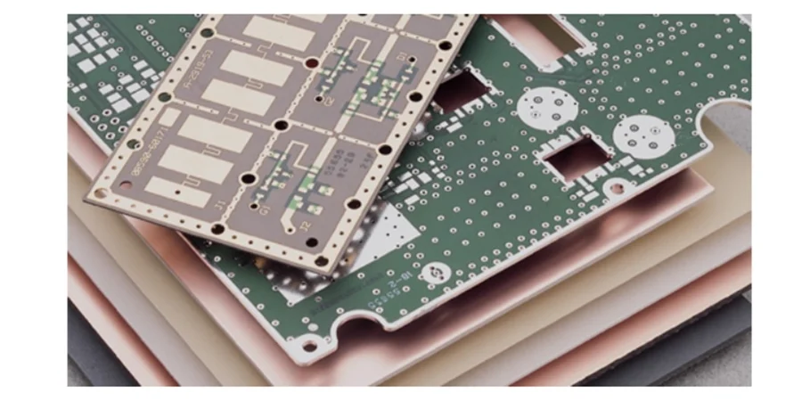
2. Hybrid Stack-Up Strategies
- Cost and Performance Balance: Fully PTFE boards offer the best performance but at higher cost. A hybrid structure-PTFE for RF layers and FR-4 or hydrocarbon-ceramic materials (e.g., Rogers 4003C) for lower-frequency or digital layers-is often optimal.
- Thermal Expansion Matching: When mixing materials, select prepregs with compatible coefficients of thermal expansion (CTE) to prevent delamination or via cracking during thermal cycling.
- Lamination Process: Hybrid boards require careful lamination sequencing, pressure, and temperature control. Always consult the material manufacturer’s datasheet for lamination profiles specific to PTFE-based composites.
3. Via and Transition Design
- Via Stubs: Avoid or back-drill stubs on high-frequency transmission lines to minimize signal reflection.
- Via Plating: Ensure sufficient copper thickness and uniform plating, as PTFE’s low adhesion can challenge via reliability.
- Via-to-Trace Transition: Taper the pad-to-trace junction or use anti-pad clearance optimization to minimize impedance discontinuities.
- Grounded Vias: Implement via fences or via stitching alongside RF traces for controlled impedance and EMI shielding.
4. Copper Foil and Conductor Choices
- Type Selection: For frequencies above 10 GHz, use very low profile (VLP) or rolled annealed copper to reduce insertion loss.
- Thickness: Typical values are ½ oz (17 µm) or 1 oz (35 µm). Thicker copper increases conductor loss and affects impedance control.
- Plating Considerations: Maintain uniform plating in high-density regions to avoid impedance mismatch between plated and unplated areas.
5. Surface Finishes for RF Compatibility
- Preferred Finishes:
- ENIG (Electroless Nickel Immersion Gold): Stable and solderable; adds minimal surface roughness, suitable for most RF circuits.
- ENEPIG (Electroless Nickel Electroless Palladium Immersion Gold): Offers superior wire-bonding and oxidation resistance.
- Immersion Silver: Excellent conductivity and flatness; ideal for high-frequency lines but requires careful handling to prevent tarnishing.
- Avoid HASL: Hot Air Solder Leveling creates uneven surface topography and variable thickness that disturb impedance control.
6. Grounding, Shielding, and Layout Practices
- Ground Plane Integrity: Use solid, uninterrupted planes for return currents. Stitch grounds with vias around signal paths to prevent radiation and crosstalk.
- Component Placement: Place sensitive RF components close to connectors and minimize trace length. Keep power circuits isolated from signal paths.
- Trace Bends: Use gentle curves or mitered bends instead of sharp 90° corners to reduce signal reflection.
7. Thermal Management
- Material Conductivity: PTFE has low thermal conductivity (0.25-0.6 W/m·K). Where possible, use thermal vias, copper planes, or embedded metal cores for heat dissipation.
- Component Spacing: Maintain adequate spacing around high-power amplifiers or oscillators to prevent localized heating and detuning.
8. Material Handling and Process Compatibility
- Drilling and Routing: PTFE is soft and elastic; use sharp, diamond-coated tools and optimized feed rates to avoid burrs and smearing.
- Surface Preparation: Chemical etching or plasma treatment before copper cladding enhances adhesion.
- Storage Conditions: PTFE absorbs almost no moisture, but hybrid materials may-store and pre-bake before lamination or reflow soldering.
Following these guidelines ensures your PTFE circuit boards achieve consistent impedance, low loss, and long-term reliability even at millimeter-wave frequencies (24 GHz, 77 GHz, and beyond). When combined with rigorous simulation, controlled fabrication, and precision assembly, they form the backbone of advanced RF and microwave systems.
Ensuring Performance: Our Rigorous Testing and Quality Assurance Protocol {#quality-assurance}
To guarantee that every PTFE circuit board meets its performance specifications, HILPCB implements a multi-level testing protocol:
- Automated Optical Inspection (AOI): Verifies trace geometry and registration accuracy.
- Impedance and S-Parameter Testing: We use a network analyzer to confirm transmission line performance and signal integrity.
- Microsection Analysis: We physically cross-section test coupons to evaluate plating quality and layer-to-layer bonding.
- Thermal Cycling: Simulates real-world operating conditions to validate reliability for demanding aerospace and automotive applications.
This rigorous approach is central to our PTFE PCB manufacturing process, ensuring you receive a product you can trust.