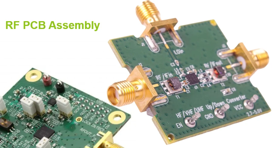
Die RF-Leiterplattenbestückung stellt einzigartige Herausforderungen dar, die sie von der konventionellen Elektronikbestückung unterscheiden. Hochfrequenzschaltungen erfordern eine präzise Bauteilplatzierung, spezielle Löttechniken und sorgfältige Beachtung parasitärer Effekte, die bei niedrigeren Frequenzen unbedeutend wären. Erfolg erfordert das Verständnis sowohl der elektrischen als auch der mechanischen Aspekte der RF-Komponentenintegration.
Bei Highleap PCB Factory haben wir Montageprozesse entwickelt, die speziell für RF-Anwendungen von DC bis 77 GHz optimiert sind. Unser Ansatz kombiniert Präzisionsplatzierungsgeräte, kontrollierte Temperaturprofile und umfassende Tests, um sicherzustellen, dass Ihre RF-Designs ihr volles Leistungspotenzial ausschöpfen.
RF-Komponenteneigenschaften und Handhabung
Bei RF-Komponenten ist Präzision entscheidend. Im Gegensatz zu digitalen Komponenten erfordern RF-Teile eine spezielle Handhabung, um Spitzenleistung zu gewährleisten. Hier ist, warum unser Ansatz zur RF-Komponentenhandhabung hervorsticht:
- Hervorragende Verpackung: Wir verwenden fortschrittliche Verpackungslösungen wie QFN, die parasitäre Induktivität und Kapazität minimieren. Dies führt zu überlegener RF-Leistung mit präziser Platzierung und Wärmemanagement, die bei der Montage den Unterschied ausmachen.
- Optimale Komponentenausrichtung: Jede RF-Komponente hat spezifische Ausrichtungsanforderungen, um den Signalfluss und die Leistung zu optimieren. Durch Befolgen detaillierter Platzierungsanweisungen stellen wir sicher, dass jede Komponente für maximale Effizienz positioniert ist.
- Fortgeschrittene parasitäre Effektsteuerung: Selbst die kleinsten Komponenten können die Stabilität Ihrer Schaltung beeinflussen. Unsere strenge Platzierungstoleranz (±0,05 mm) stellt sicher, dass parasitäre Effekte innerhalb der Entwurfsgrenzen bleiben und die Integrität Ihrer Schaltung erhalten bleibt.
- Schutz Ihrer Investition: RF-Komponenten sind empfindlich gegenüber Umwelteinflüssen wie ESD und Feuchtigkeit. Unsere kontrollierten Montageumgebungen mit ESD-Schutz und Feuchtigkeitskontrolle verhindern Schäden und gewährleisten lang anhaltende Leistung.
Bei jedem Schritt stellt unser Handhabungsprozess sicher, dass Ihre RF-Komponenten mit der Sorgfalt behandelt werden, die sie verdienen, um Ihre Investition zu schützen und die Leistung zu optimieren.
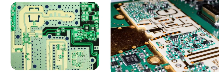
Präzise Montageprozesse
Montagepräzisionsfähigkeiten
RF assembly demands precision that exceeds typical surface mount requirements. Component placement accuracy directly affects circuit performance through parasitic effects and impedance matching.
Pick and place precision utilizes advanced vision systems and precision mechanical systems to achieve ±0.05mm placement accuracy. This precision ensures that component parasitics remain within design tolerances while maintaining proper impedance matching for critical RF paths.
Stencil design optimization controls solder paste application for consistent joint formation. RF components often require specialized stencil apertures to account for different thermal masses and joint requirements compared to digital components.
Reflow profiling uses carefully controlled thermal cycles optimized for RF materials and components. Many RF substrates have lower maximum processing temperatures than standard FR4, requiring modified reflow profiles that balance joint reliability with substrate integrity.
Fine pitch capability handles the increasing miniaturization of RF components. We routinely assemble components with 0.4mm pitch while maintaining high yield and reliability standards.
The precision assembly process ensures that the electrical performance designed into the PCB is preserved through the assembly operations.
RF PCB Assembly Best Practices
Achieving success in RF PCB assembly requires more than just technical precision—it demands a strategy that balances cost efficiency, speed, and quality assurance. By focusing on these three pillars, you can reduce overall project expenses, shorten delivery cycles, and ensure your RF designs perform reliably under real-world conditions.
💰 Cost Efficiency
- Mixed-Material Usage: Apply high-frequency laminates (e.g., Rogers, Taconic) only where needed, use FR-4 elsewhere to reduce cost without sacrificing performance.
- Panel Optimization: Maximize board utilization per panel to lower material waste and cut per-unit cost.
- Early DFA Reviews: Catch layout or footprint issues before production to avoid re-spins and wasted materials.
⏱ Time Savings
- Rapid Prototyping: Automated SMT lines with ±0.05mm accuracy ensure quick turnaround for prototypes, even with 01005 components.
- Streamlined Workflows: Pre-defined thermal profiles and optimized placement sequences shorten assembly time without compromising yield.
- Express Options: 3–5 day assembly available for urgent projects to accelerate time-to-market.
✔️ Quality Assurance
- Controlled Atmosphere Reflow: Stable solder joints with minimal thermal stress for sensitive RF components.
- AOI & X-ray: 100% inspection including hidden joints under BGAs/QFNs to guarantee reliability.
- RF Performance Testing: Impedance, insertion loss, and return loss verified using VNAs up to 77GHz.
Quality Control and Testing
Automated Optical Inspection (AOI)
Provides 100% inspection coverage for component placement, orientation, and solder joint quality using advanced algorithms trained for RF component recognition and defect detection.
X-ray Inspection
Reveals hidden defects in BGA and QFN components that optical inspection cannot detect, crucial for RF power amplifiers and other critical components where joint defects could lead to catastrophic failures.
In-circuit Testing
Validates basic electrical connectivity and component values. While full RF performance testing requires specialized equipment, in-circuit testing can quickly identify major assembly defects cost-effectively.
RF Performance Testing
Validates critical electrical parameters using network analyzers and RF test equipment, ensuring key performance metrics like gain, return loss, and isolation meet specification requirements.
Functional Testing
Validates overall system performance under actual operating conditions, often revealing system-level issues that component-level testing cannot detect.
Environmental Stress Testing
Simulates extreme conditions (e.g., temperature, humidity) to verify product robustness and ensure it operates under a wide range of environmental factors.
Optimized RF PCB Assembly for Scalable Production
When scaling RF PCB assembly from prototype to full production, it's essential to optimize both performance and cost. We help you achieve the perfect balance between high-quality assembly, cost-effectiveness, and efficient throughput.
Consistent Assembly Standards: We standardize all critical processes to ensure every RF PCB assembly meets precise specifications, regardless of production volume. This consistency guarantees high-quality results every time, no matter the scale.
Minimized Defects and Maximized Yield: Our specialized focus on RF PCB assembly allows us to identify and eliminate defects that uniquely affect RF components. With targeted analysis and custom corrective actions, we enhance yields and reduce costly rework.
Efficient Equipment and Technology: Our advanced equipment is optimized for RF PCB assembly, ensuring that your designs are produced efficiently without sacrificing quality. We keep our assembly lines flexible to accommodate the variety of RF components used in your circuits.
Expert Supply Chain Management: Sourcing and managing RF components can be complex, with longer lead times and specialized requirements. We have established strong relationships with trusted RF suppliers and employ efficient inventory management to keep your production on schedule.
Accurate Cost Modeling for RF Assembly: We provide clear and precise cost breakdowns for every stage of the RF PCB assembly process. Our cost modeling ensures competitive pricing, offering you value without compromising on the quality and reliability your product needs.
Why Choose Our RF PCB Assembly Services?
Our experience in RF PCB assembly ensures your projects are built with the precision required for high-frequency applications while achieving cost and throughput targets. By focusing on both the technical and financial aspects of RF assembly, we help bring your products to market faster, more efficiently, and within budget.
Ready to scale your RF PCB assembly without compromising on performance or cost? Let our expert team streamline your production process to ensure your designs meet the highest standards at competitive prices. Contact us today to learn more!
Expert RF Assembly Services
Precision assembly from prototype through production volumes
Request Assembly QuoteIntegrated Services: RF PCB Impedance Control | RF PCB Materials | RF PCB Testing