
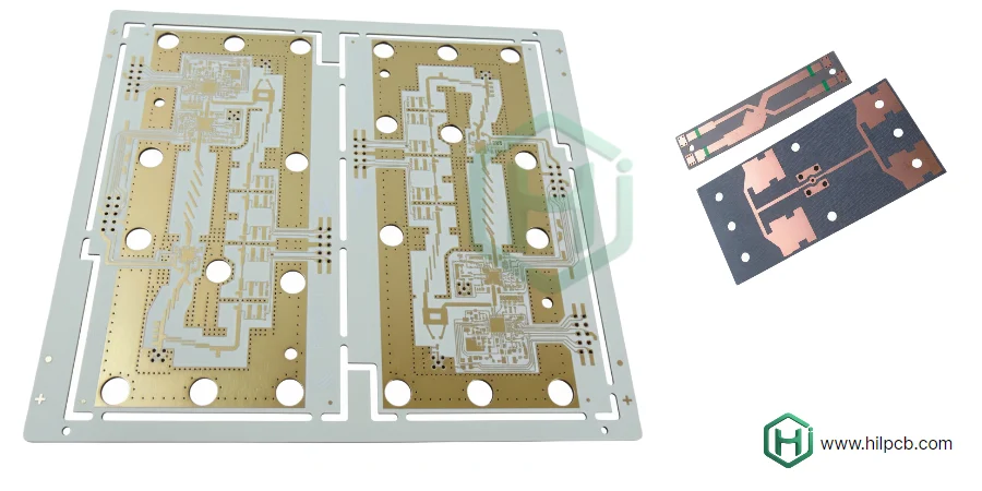
As signal speeds enter the gigabit-per-second (Gbps) era and operating frequencies climb into the gigahertz (GHz) range, standard FR-4 PCB material is no longer a viable option. Signals traveling through FR-4 at these speeds suffer severe degradation, much like water flowing through a leaky pipe. A Low Loss PCB is the solution, engineered with advanced dielectric materials to minimize this signal attenuation and ensure total signal integrity.
This guide provides a clear framework to help you understand what a low loss PCB is, how to select the right material for your specific application, and the critical design and manufacturing points you need to consider.
What is a Low Loss PCB, and Why is it Critical? {#what-is-a-low-loss-pcb}
Simply put, a low loss PCB is a circuit board made with a special insulating material (dielectric substrate) that significantly reduces the loss of electrical energy as a signal travels through it.
This signal loss primarily comes from two sources:
- Dielectric Loss: This is the main contributor to loss at high frequencies. As the signal's electromagnetic field passes through the substrate, some of its energy is absorbed by the material and converted into heat, weakening the signal.
- Conductor Loss: This is caused by the resistance of the copper traces, as well as the "skin effect" and copper surface roughness at high frequencies.
You need to consider a low loss PCB if your design involves any of the following:
- High-Speed Digital Circuits (e.g., 28 Gbps, 56 Gbps, 112 Gbps)
- RF/Microwave Applications (e.g., 5G communications, radar, satellite)
- Long-Distance Signal Traces (e.g., large backplanes, long cable drivers)
- Systems with strict requirements for jitter and eye-diagram opening
How to Choose the Right Low Loss PCB Material {#choosing-your-material}
"Low loss" is not a single material but a spectrum of options with varying performance and cost. To simplify the selection process, we have categorized common low loss materials into three tiers, allowing you to choose based on your application's frequency, performance needs, and budget.
Tier 1: High-Performance FR-4 - The Entry-Level Low Loss Solution
This is the "entry-level" low loss category, representing an improvement over standard FR-4. These materials use an optimized resin system to achieve a lower Dissipation Factor (Df) than their conventional counterparts.
- Typical Df (@10 GHz): 0.010 - 0.015
- Typical Dk: 3.8 - 4.2
- Core Advantage: Cost-effective and compatible with standard FR-4 processing, making them easy to manufacture.
- Best For: Cost-sensitive applications operating below 5 GHz, such as entry-level servers and high-speed interfaces in consumer electronics (e.g., PCIe 3.0/4.0).
- Limitation: The loss is still too high for more demanding high-speed or RF applications beyond the 5-10 GHz range.
Tier 2: Hydrocarbon / PPO / PPE Blends - The Workhorse of High-Speed Digital
This tier of materials is specifically engineered for high-speed digital and mid-to-high frequency RF applications. They are typically based on hydrocarbon or polyphenylene oxide (PPO/PPE) resin systems, often with ceramic fillers to optimize performance.
- Typical Df (@10 GHz): 0.004 - 0.008
- Typical Dk: 3.3 - 3.8
- Representative Materials: Megtron 6, Isola I-Speed, Tachyon 100G
- Core Advantage: Provides excellent signal integrity up to 20-30 GHz, making it the go-to choice for modern high-speed digital designs (e.g., 56/112 Gbps PAM4).
- Best For: High-speed networking equipment, data center switches, server backplanes, and high-end test instruments.
- Limitation: More expensive than high-performance FR-4 and requires a higher degree of manufacturing process control.
Tier 3: PTFE-Based Substrates (Teflon) - The Gold Standard for RF & Microwave
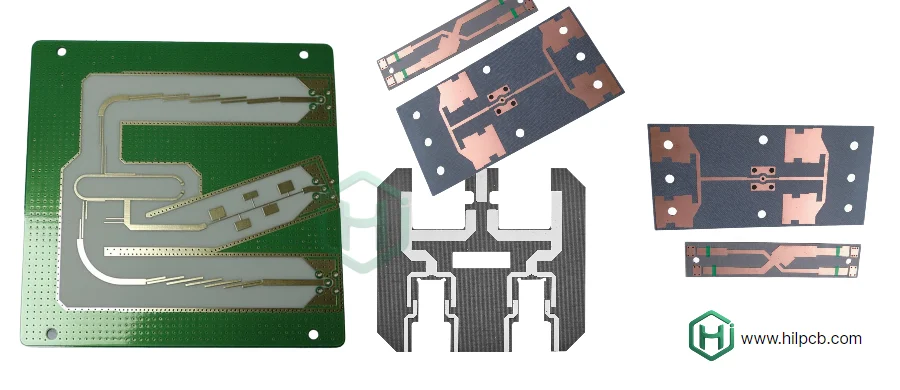
This is the pinnacle of performance. Materials based on PTFE (Polytetrafluoroethylene), widely known as Teflon™ circuit boards, offer the lowest Dissipation Factor available in any laminate. They are typically compounded with woven glass or ceramic fillers to improve mechanical stability.
- Typical Df (@10 GHz): < 0.004 (often 0.0015 - 0.003)
- Typical Dk: 2.1 - 3.0
- Core Advantage: Unbeatable low loss performance and an extremely stable dielectric constant, making it the irreplaceable choice for microwave and millimeter-wave applications.
- Best For: High frequency PTFE PCB for applications like automotive radar (77 GHz), 5G millimeter-wave antennas, satellite PTFE PCB communications, and aerospace systems.
- Limitation: The highest cost. The material is soft, making the PTFE PCB manufacturing process complex and highly demanding on the fabricator's technical capabilities.
Quick Reference Material Selection Chart
| Tier | Typical Material | Dissipation Factor (Df) | Usable Frequency | Cost | Key Applications |
|---|---|---|---|---|---|
| Entry-Level | High-Perf. FR-4 | Medium | < 5-10 GHz | Low | Servers, Consumer |
| Workhorse | Megtron 6, I-Speed | Low | < 20-30 GHz | Medium | Data Centers, High-Speed Digital |
| Gold Standard | PTFE (Teflon) | Ultra-Low | > 20 GHz | High | Radar, 5G mmWave, Satellite |
Key Design Techniques to Minimize Signal Loss {#key-design-techniques}
Choosing the right material is half the battle. Excellent design practices can reduce loss even further:
- Use Smoother Copper Foil: At high frequencies, signals travel on the copper surface (skin effect). Rough copper increases the path length and thus the loss. Specifying very-low-profile (VLP) copper is crucial.
- Keep Traces Short and Direct: The most straightforward way to reduce loss is to reduce the distance the signal travels.
- Optimize Vias: The unused portion of a via (stub) can create resonant reflections at specific frequencies, causing massive signal loss. Back-drilling is often used to remove them.
- Ensure a Solid Return Path: Avoid splits or gaps in the ground plane directly beneath your signal traces.
Why Manufacturing Precision is Critical for Low Loss PCBs {#why-manufacturing-precision-is-critical}
A perfect design can be ruined by poor manufacturing. For low loss PCBs, tight control over manufacturing tolerances is absolutely essential.
- Dielectric Thickness Control: Variations in the thickness between a trace and its ground plane will directly alter its impedance.
- Trace Width and Spacing: The etching process must be extremely precise to maintain the designed trace geometry.
- Lamination and Drilling: Improper processing, especially with soft materials like PTFE, can lead to delamination or poor hole-wall quality.
At HILPCB, we use advanced equipment and strict process controls, such as plasma treatment, laser drilling, and Automated Optical Inspection (AOI), to ensure every Teflon PCB product is fabricated precisely to its design specifications.
For high-performance applications where signal integrity cannot be compromised, partnering with a manufacturer who understands both the science of low loss materials and the art of precision fabrication is the key to success.
Frequently Asked Questions About Low Loss PCBs {#faq}
What is the difference between dielectric constant (Dk) and dissipation factor (Df)?
While both are critical, they measure different things. The Dielectric Constant (Dk) primarily affects impedance and the speed at which a signal travels. The Dissipation Factor (Df), or loss tangent, directly measures how much signal energy is absorbed and lost as heat within the material. For "low loss," a low Df is the most important property.
At what frequency is a low loss PCB necessary instead of FR-4?
There is no single answer, as it depends on the trace length and the total acceptable loss for your system (your "loss budget"). However, a general rule of thumb is that standard FR-4 becomes problematic for most applications operating above 2-3 GHz. For longer traces or more sensitive systems, the need for a low loss material may arise at even lower frequencies.
How does the cost of low loss materials compare to standard FR-4?
There is a significant cost difference. As a rough estimate, a high-performance FR-4 (Tier 1) might cost 1.5-2 times more than standard FR-4. A Tier 2 material like Megtron 6 could be 3-5 times the cost. The highest performance Tier 3 PTFE materials can be 5-10 times the cost of FR-4, or even more, depending on the specific type.
How does copper roughness affect signal loss in a PCB?
At high frequencies, current travels only on the outer "skin" of a copper trace (the skin effect). If the copper surface is rough, the signal has to travel a longer, more winding path, which increases resistance and therefore increases the conductor loss. Using smooth, very-low-profile (VLP) copper foil is a key strategy to minimize this effect.
Can you mix low loss and standard FR-4 materials in a hybrid PCB stack-up?
Yes, this is a common and effective cost-saving strategy. For example, the critical high-speed or RF signals can be routed on outer layers made from a low loss material, while the inner layers used for power and low-speed signals can be standard FR-4. This "hybrid" or "mixed-dielectric" approach requires an experienced manufacturer like HILPCB to manage the different material properties during the lamination process.