
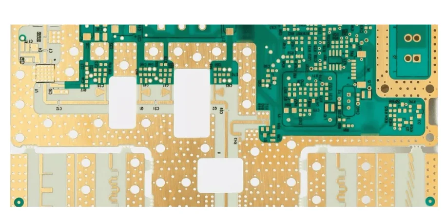
When operating in the multi-GHz frequency range, standard PCB materials no longer provide the necessary performance. PTFE PCB manufacturing offers a solution for ultra-low-loss, high-integrity boards-but only when material selection, design, and manufacturing processes are aligned.
This guide provides engineers, system architects, and procurement teams with the knowledge to make informed decisions about:
- The importance of PTFE circuit boards for RF and high-frequency applications.
- How to select the correct PTFE material for your system.
- Key Design-for-Manufacturability (DFM) practices for successful PTFE PCB fabrication.
- An inside look at the advanced PTFE PCB manufacturing process.
- How to choose a reliable and experienced PTFE PCB manufacturer.
- The benefits of integrated PCB and assembly solutions to minimize risk.
Table of Contents
- Why PTFE PCBs Matter for High-Frequency Systems
- Material Selection for PTFE PCB Manufacturing
- Design-for-Manufacturability (DFM): Ensuring Success
- PTFE PCB Manufacturing Process
- Choosing the Right PTFE PCB Manufacturer
- Applications of PTFE PCBs
- Conclusion
Why PTFE PCBs Matter for High-Frequency Systems
Standard PCB materials (e.g., FR-4) cannot meet the performance demands for high-frequency and RF PCB applications, which require low-loss, stable signal transmission. PTFE offers key advantages:
- Low Dielectric Loss: PTFE laminates significantly reduce signal attenuation, which is critical for preserving signal integrity in RF/microwave systems.
- Stability Over Frequency: Unlike traditional materials, PTFE maintains a stable dielectric constant (Dk) across a wide range of frequencies, preventing phase distortion.
- Superior Performance at GHz Frequencies: At high frequencies, copper conductor losses dominate, but PTFE offers the necessary material properties to mitigate this issue.
- Environmental Robustness: PTFE performs better in extreme environments such as aerospace, satellites, and radar systems, handling thermal cycling, vibration, and moisture with ease.
In short, PTFE PCB manufacturing is essential when reliability and performance at high frequencies are non-negotiable.
For the manufacturing handoff, review the Teflon PCB process scope and the PCB quality evidence guide alongside the material grade, stackup, and inspection requirements.
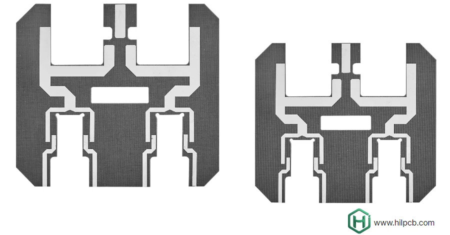
Material Selection for PTFE PCB Manufacturing
Choosing the right PTFE material is vital for achieving the best performance. Here are the most common variants and their advantages:
| Variant | Core Advantage | Manufacturing Consideration | Typical Df (@10 GHz) | Best Use Case |
|---|---|---|---|---|
| Woven-Glass Reinforced PTFE | Balanced cost & performance | Glass weave → microscopic Dk variation | ~0.001-0.002 | RF/microwave up to ~20 GHz |
| Ceramic-Filled PTFE | Ultra-low loss, stable Dk, improved thermal | Abrasive, harder drilling/plating | ~0.001-0.0015 | mmWave, avionics, radar |
| Pure (Un-reinforced) PTFE | Lowest Dk, fastest signal paths | Soft, high CTE, difficult multilayer | <0.001 | Specialized delay lines, ultra-high speed |
Key questions to ask your manufacturer:
- What laminate grades do you carry, and what are their true Dk/Df values at target frequencies?
- What types of copper foil are used? (Very-Low-Profile, Reverse-Treated?)
- How experienced is the manufacturer with PTFE stack-ups, via plating, and dielectric adhesion?
Choosing the wrong material or cutting corners during manufacturing will lead to poor performance and higher costs.
Design-for-Manufacturability (DFM): Ensuring Success
The DFM phase is where many PTFE PCB designs either succeed or fail. Here are key considerations:
- Impedance Control & Stack-up Precision: Use electromagnetic field solvers to ensure accurate impedance matching.
- Copper Foil & Surface Treatment: Specify VLP or RTF copper foils for minimal surface roughness and lower conductor loss.
- Via Design & Stub Elimination: Minimize via stubs and use blind/buried vias to reduce signal reflection.
- Return Path Integrity: Ensure ground/reference planes are continuous and well-stitched.
- Hybrid Stack-ups: Cost-effective solutions using PTFE for RF layers and FR-4 for control layers.
- Thermal & Mechanical Considerations: PTFE variants have high CTE; proper drill strategy and lamination profiles are essential.
A thorough DFM process prevents issues that could arise during fabrication and ensures the high-frequency performance of the final board.
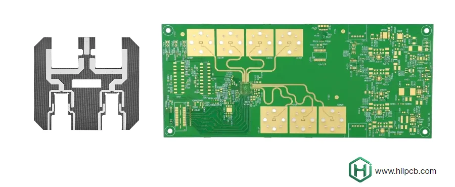
PTFE PCB Manufacturing Process
Here’s a look inside the advanced PTFE PCB manufacturing process:
- Surface Preparation: Plasma activation or chemical etching roughens the PTFE surface for copper bonding.
- Copper Cladding & Plating: Proper copper foil selection and plating ensure reliable adhesion and integrity.
- Precision Drilling & De-smear: Special drill bits and plasma de-smear ensure precise vias.
- Controlled Lamination: Vacuum lamination ensures reliable bonding with no voids or stress.
- Surface Finish & Assembly Prep: ENIG or immersion silver/tin finishes are ideal for high-frequency reliability.
- Testing & Quality Validation: TDR testing for impedance, VNA for insertion/return loss, and environmental testing ensure mission-critical reliability.
This meticulous process guarantees performance, reliability, and consistency in the final product.
PTFE PCB Manufacturing Process
PTFE printed circuit board manufacture adds three process steps that do not exist for hydrocarbon PCB systems: surface activation, staged lamination, and low-Df coupon verification. PTFE's chemical inertness means a standard FR-4 desmear will not produce reliable hole-wall adhesion; plasma activation is required to lift surface energy before electroless copper can bond. Staged lamination keeps the bonding film below its flow temperature until the alignment of the stack is locked, which prevents the resin-rich areas that distort impedance on PTFE cores.
The key manufacturing stages:
| Stage | Process control | Why it matters for PTFE PCB manufacture |
|---|---|---|
| Surface prep | Plasma activation (O₂/CF₄ chemistry) | Raises surface energy for hole-wall adhesion >1.0 N/mm |
| Lamination | Staged pressure/temperature, 175–185 °C, slow cool-down | Prevents bondline voiding and layer shift |
| Drilling | Carbide bits, controlled infeed, depth control | Avoids smear that masks copper-to-substrate bond |
| Plating | Electroless + electrolytic copper, low-stress chemistry | Compensates for PTFE's high Z-axis expansion |
| Surface finish | ENIG, ImmAg, or OSP per design | Controls solderability and wire-bond compatibility |
| Verification | TDR impedance, microsection, optional VNA | Confirms electrical and physical build matches RFQ |
Most PTFE printed circuit board manufacture failures can be traced to one of these stages being treated as FR-4: a typical symptom is via-pull or delamination during reflow, or impedance drifting out of tolerance on the first few panels of a build. Asking the manufacturer for a PTFE-specific process map and a first-article cross-section report is the cheapest way to avoid the second spin.
For programs that mix PTFE on RF layers and FR-4 on digital/power layers (the hybrid stackup reviewed in Teflon/PTFE PCB), the same activation and lamination logic applies to the bonding film between the PTFE cores and the FR-4 prepreg. Material compatibility, CTE matching, and bondline thickness should all be reviewed together; do not assume a hybrid stack inherits PTFE's process latitude on the FR-4 side.
Choosing the Right PTFE PCB Manufacturer
A qualified PTFE PCB manufacturer must have:
- Expertise in high-frequency and RF PCB fabrication.
- Experience with advanced PTFE laminates and high-precision fabrication methods.
- In-house testing capabilities (TDR, VNA) for transparent performance reporting.
- Certifications like AS9100 or ISO 9001 that align with aerospace, defense, or commercial RF applications.
A manufacturer without this experience can lead to costly delays, poor yields, and compromised performance.
Applications of PTFE PCBs
PTFE PCBs are essential in high-performance, high-reliability applications, including:
- Satellite communications
- Aerospace systems & payloads
- Radar systems and military RF modules
- 5G/6G mmWave infrastructure
- High-speed data links (25 Gbps, 56 Gbps, 112 Gbps)
- Precision test equipment
- Low-loss PCBs for mission-critical RF paths
PTFE is not just for performance-it’s a critical part of ensuring long-term system reliability and low-latency communication in these applications.
Conclusion
Investing in PTFE PCB manufacturing is crucial for achieving the highest performance in high-frequency, mission-critical systems. Whether it’s RF, microwave, or high-speed applications, the right PTFE materials and precise manufacturing ensure minimal signal loss, phase stability, and long-term reliability.
A successful PTFE PCB process involves selecting the appropriate laminate, adhering to Design-for-Manufacturability (DFM) principles, and partnering with an experienced manufacturer. These elements directly affect your system's performance and production efficiency.
If executed properly, PTFE PCB technology unlocks ultra-low loss and stable signal integrity, which are essential for high-performance applications. However, neglecting any of these aspects can lead to costly delays, reduced quality, and underperformance.
For your next high-frequency or mission-critical project, treat PTFE PCB manufacturing as a strategic element of your design, not a secondary consideration. Choosing the right materials, design strategies, and a trusted manufacturing partner is the key to achieving success.