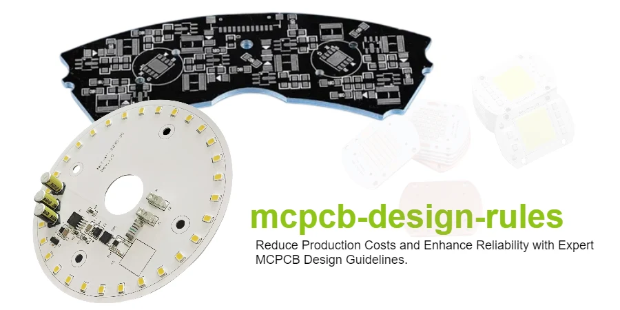
At Highleap PCB Factory, we've refined MCPCB design rules through manufacturing over 10,000 metal core PCB projects. This comprehensive guide provides engineers with proven design strategies, manufacturing constraints, and optimization techniques that ensure first-pass success. Whether designing LED lighting, power electronics, or automotive systems, these guidelines transform thermal challenges into reliable, manufacturable solutions.
MCPCB Design Specifications and Basic Requirements
Understanding fundamental MCPCB design constraints forms the foundation for successful thermal management boards. Metal core PCBs operate under different rules than traditional FR-4, requiring specialized knowledge to avoid common pitfalls that lead to manufacturing delays or field failures.
Layer Stack-up Configuration: Single-layer MCPCB represents 90% of applications, consisting of copper circuit (35-420μm), dielectric layer (75-150μm), and metal substrate (0.5-3.0mm). The dielectric layer cannot be drilled through, eliminating plated through-holes in single-layer designs. Double-layer MCPCB exists but costs 2-3x more, requiring special processing for limited applications. Multi-layer constructions combine MCPCB with traditional PCB layers for complex circuits requiring thermal management.
Dielectric Material Selection: The thermally conductive dielectric layer balances electrical isolation with heat transfer, determining overall thermal performance. Standard 1.0 W/m·K materials cost least, suitable for general LED applications under 5W. Enhanced 2.0-3.0 W/m·K dielectrics handle automotive and industrial power applications. Premium 5.0-8.0 W/m·K formulations address extreme thermal challenges but cost 2-3x standard. Temperature rating typically 130-150°C continuous, with some materials rated to 180°C. Breakdown voltage ranges from 1000V to 4000V depending on thickness and formulation.
Substrate Material Options: Aluminum PCB substrates dominate with 95% market share due to optimal cost-performance balance. 5052 alloy offers good formability and 140 W/m·K conductivity for most applications. 6061 alloy provides higher strength and 167 W/m·K for demanding environments. 1100 pure aluminum achieves maximum 220 W/m·K for extreme thermal requirements. Copper core PCB substrates deliver 385 W/m·K but cost 3-4x aluminum, reserved for special applications.
MCPCB Design Rule Summary
| Parameter | Minimum | Standard | Advanced |
|---|---|---|---|
| Trace Width/Space | 0.15/0.15mm | 0.20/0.20mm | 0.10/0.10mm |
| Via Diameter | 0.3mm | 0.5mm | 0.2mm |
| Edge Clearance | 0.5mm | 1.0mm | 2.0mm (HV) |
| Annular Ring | 0.10mm | 0.15mm | 0.20mm |
| Solder Mask Dam | 0.08mm | 0.10mm | 0.15mm |
Electrical Isolation Requirements: Voltage isolation depends on dielectric thickness and material properties requiring careful specification. Creepage distance calculations follow IPC-2221 standards with modifications for metal substrates. 1000V applications require 0.2mm minimum conductor spacing for pollution degree 2. 2500V applications need 0.5mm spacing with consideration for altitude derating. 4000V designs demand 1.0mm minimum with specialized high-voltage dielectrics. Safety factor of 2x recommended for automotive and industrial applications ensuring long-term reliability.
Mechanical Design Constraints: Board outline geometry impacts manufacturability and reliability throughout product lifetime. Minimum board size 10×10mm limited by handling and processing equipment. Maximum single piece 600×500mm, larger sizes require step-and-repeat panelization. Corner radius minimum R0.5mm prevents stress concentration and cracking. Mounting holes typically non-plated with 0.5mm wall to copper minimum. Thickness tolerance ±10% standard, ±5% achievable with controlled processes.
MCPCB Thermal Management Design Techniques
Effective thermal management design transforms MCPCB from simple substrate to sophisticated heat dissipation system. These techniques, validated through thermal simulation and real-world testing, ensure components operate within safe temperature limits while maximizing reliability.
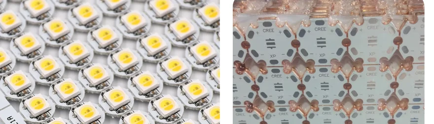
Thermal Via Strategy and Optimization: Thermal vias create critical heat transfer paths from hot components to the metal substrate below. Via placement directly under heat sources reduces thermal resistance 50-70% compared to lateral conduction alone. Optimal via diameter of 0.3-0.5mm balances thermal performance with manufacturing cost and reliability. Via arrays with 1.0-1.5mm pitch provide distributed heat transfer for large components. Filled vias using copper plating or thermal epoxy prevent solder wicking and improve thermal performance 30%. Calculate array thermal resistance: Rth_array = Rth_single / (n × η) where η is efficiency factor (0.6-0.8).
Copper Coverage and Distribution: Maximizing copper coverage enhances lateral heat spreading before reaching the substrate. Target 70-85% copper coverage for optimal thermal performance without excessive material cost. Solid copper floods under high-power components create thermal spreading planes. Thermal highways 2-5mm wide connect heat sources to board edges or cooling zones. Mesh patterns maintain coverage while reducing weight for portable applications. Avoid isolated copper islands larger than 25mm² that create thermal dead zones.
Component Placement for Thermal Optimization: Strategic component positioning prevents thermal interactions ensuring reliable operation. Power density mapping identifies hot zones requiring special attention—maintain <10W/cm² for natural convection. Separation distance of 5-10mm between major heat sources prevents thermal coupling. Temperature-sensitive components placed >15mm from heat sources or in dedicated cool zones. Edge placement for high-power devices maximizes heat dissipation to ambient. Staggered arrangement promotes convection airflow between components.
Thermal Via Design Calculator
Single Via Thermal Resistance
Formula: Rth = L/(k×π×r²)
0.3mm via: ~50°C/W (unfilled)
0.5mm via: ~30°C/W (unfilled)
Filled: 30-40% improvement
Via Array Performance
3×3 array: Rth ÷ 7.2
5×5 array: Rth ÷ 20
7×7 array: Rth ÷ 39
10×10 array: Rth ÷ 80
Optimal Spacing
Minimum: 0.5mm edge-to-edge
Standard: 1.0-1.5mm pitch
Power devices: Full coverage
LED arrays: Under each die
Cost Impact
Standard via: Base cost
Filled via: +15-20%
Cu filled: +30-40%
Via-in-pad: +25%
Thermal Zone Management: Dividing the board into thermal zones enables optimized cooling strategies for different power densities. Hot zones (>10W/cm²) require maximum thermal vias, copper coverage, and edge proximity. Warm zones (5-10W/cm²) need moderate thermal management with standard via patterns. Cool zones (<5W/cm²) house sensitive components with minimal thermal features for cost optimization. Thermal barriers using routed slots or reduced copper create isolation between zones. Thermal bridges with heavy copper or filled vias channel heat to specific cooling points.
Heat Sink Integration Design: Direct coupling to external heat sinks multiplies MCPCB cooling capacity for extreme applications. Mounting boss areas require exposed metal substrate for optimal thermal interface. Thermal interface materials (TIM) selection impacts overall thermal resistance significantly. Pressure-sensitive adhesive TIMs simplify assembly but add 0.5-1.0°C/W resistance. Phase-change materials optimize contact at operating temperature reducing resistance 30%. Spring-loaded mounting ensures consistent pressure across temperature ranges.
MCPCB Trace Routing and Copper Design
Electrical routing on MCPCB follows modified rules accounting for thermal and mechanical constraints unique to metal substrates. Proper trace design ensures current capacity, signal integrity, and manufacturing yield while maintaining thermal performance objectives.
Current Capacity Calculations: MCPCB traces handle higher current than FR-4 due to superior heat dissipation from the metal substrate. For 20°C rise above ambient: 1oz copper requires 0.25mm/amp, 2oz needs 0.15mm/amp, 3oz handles 0.10mm/amp. Derate by 0.7x for traces longer than 25mm due to accumulated heating effects. Parallel traces for very high currents maintain redundancy and thermal distribution. Use IPC-2152 nomographs with MCPCB-specific thermal corrections for accurate sizing.
Power Plane Design: Large copper areas serving as power distribution networks require special attention on MCPCB. Minimum 0.5mm clearance between different voltage planes prevents arcing or breakdown. Thermal relief spokes (0.3-0.5mm width) enable reliable soldering while maintaining electrical connection. Direct connection for maximum current capacity where soldering isn't required. Copper balancing between circuit and substrate sides (if double-sided) prevents warpage. Mesh patterns reduce weight while maintaining >70% coverage for thermal performance.
High-Frequency Considerations: RF and high-speed signals face unique challenges on metal substrate boards. Parasitic capacitance increases 3-5x compared to FR-4 requiring impedance adjustment. Microstrip calculations must account for dielectric properties and metal substrate effects. Keep high-frequency traces short (<50mm) and direct to minimize losses and reflections. Ground plane coupling through substrate requires careful via fence placement. Edge plating provides superior shielding for sensitive signals when required.
Copper Weight Selection Guide
| Copper Weight | Thickness | Current (1mm trace) | Applications |
|---|---|---|---|
| 1 oz | 35μm | 4A max | LED, signal circuits |
| 2 oz | 70μm | 7A max | Power supplies |
| 3 oz | 105μm | 10A max | Motor drives |
| 4+ oz | 140+μm | 13A+ max | High power |
*Current ratings assume 20°C temperature rise in 25°C ambient
Thermal Relief Patterns: Component pad connections balance electrical/thermal performance with manufacturing reliability. Four-spoke pattern (90° spacing) provides standard thermal isolation for easy soldering. Two-spoke pattern (180° spacing) offers compromise between thermal and soldering. Direct connection maximizes heat transfer but complicates manual rework. Spoke width typically 0.3-0.5mm, wider for high-current applications. Adjustment based on component thermal mass and soldering process requirements.
Solder Mask Design Rules: Solder mask on MCPCB serves both protective and functional purposes affecting performance. Mask clearance 0.05-0.10mm larger than pad ensures complete exposure for soldering. White mask for LED applications requires 20-30μm thickness for >85% reflectivity. Black mask maximizes thermal radiation adding 5-10% cooling capacity. Avoid excessive mask thickness over thermal vias reducing heat transfer efficiency. Define solder dams minimum 0.10mm between adjacent pads preventing bridging.
MCPCB Manufacturing Constraints and DFM Guidelines
Understanding manufacturing limitations during design prevents costly iterations and ensures smooth production. These Design for Manufacturing (DFM) guidelines, refined through processing millions of MCPCB boards, guarantee your design translates successfully from CAD to finished product.
Panel Utilization Optimization: Efficient panelization reduces per-unit cost by 15-30% through material optimization. Standard production panels measure 457×610mm (18"×24") or 406×508mm (16"×20"). Calculate array quantity: (Panel area - border) / (Board area + spacing). Minimum 5mm borders for handling and 2mm spacing between boards. Include fiducial marks in panel corners for automated optical alignment. Bad board marking positions enable efficient defect tracking during MCPCB assembly.
Routing and Scoring Constraints: Board separation method impacts design rules and final edge quality. V-scoring requires straight edges with 30° or 45° angle, minimum 0.8mm remaining thickness. Tab routing allows complex shapes but needs 3-5mm tabs for stability during processing. Minimum inside corner radius R0.5mm for routing, larger for thick substrates. Perforation patterns balance easy separation with handling stability. Edge plating not possible with V-scoring, plan accordingly for shielding requirements.
Hole and Cutout Specifications: Mechanical features require specific design rules for reliable manufacturing. Non-plated holes standard for MCPCB, minimum 0.5mm diameter for drilling. Plated holes possible in specialized double-sided MCPCB at significant cost premium. Countersink and counterbore available for flush mounting requirements. Slots and cutouts minimum width equals substrate thickness for stability. Maintain 0.5mm web between adjacent holes preventing breakout.
Surface Finish Selection Impact: Surface finish choice affects assembly, reliability, and cost significantly. HASL provides economical option but adds thickness variation affecting fine-pitch assembly. ENIG offers flat surface ideal for fine-pitch and aluminum wire bonding applications. OSP gives ultra-flat finish but limited shelf life and thermal cycling capability. Immersion silver balances performance and cost for most applications. Consider finish thickness in impedance calculations and mechanical clearances.
Tolerance Stack-up Management: Cumulative tolerances affect fit and function requiring careful management. Board outline ±0.20mm standard, ±0.10mm achievable with premium processing. Hole position ±0.15mm relative to board edges and each other. Thickness tolerance ±10% for substrate plus circuit layers combined. Warpage <0.7% measured diagonally for assembled boards. Feature-to-edge minimum 1mm accounting for all tolerance accumulations.
MCPCB Design Verification and Review Checklist
Comprehensive design verification before manufacturing prevents delays, reduces costs, and ensures reliable performance. This systematic review process, covering electrical, thermal, and mechanical aspects, catches issues early when corrections are simple and inexpensive. Proper verification combined with reliability testing ensures long-term performance.
Electrical Design Verification: Verify all traces meet minimum width requirements for current capacity including derating factors. Check clearances between conductors match voltage isolation requirements with safety margins. Confirm via sizes and quantities handle expected current without excessive temperature rise. Validate ground plane connectivity and return paths for all signals. Review high-voltage regions for adequate creepage and clearance distances. Test points accessible for in-circuit testing and troubleshooting.
Thermal Design Validation: Calculate junction temperatures for all heat-generating components confirming within specifications. Verify thermal via placement optimization under high-power devices using thermal modeling. Check copper coverage >70% for effective heat spreading to substrate. Confirm component placement prevents thermal interactions between heat sources. Review heat sink mounting areas for proper substrate exposure and flatness. Validate thermal interface specifications match application requirements.
Mechanical Design Check: Measure board dimensions fit within standard panel sizes for optimal material usage. Verify mounting holes positioned correctly with adequate wall thickness to copper. Check corner radii and edge clearances meet manufacturing requirements. Confirm component courtyard areas prevent mechanical interference. Review flexibility requirements for applications with vibration or flexing. Validate marking and labeling legibility with appropriate sizes and locations.
Pre-Production Review Checklist
📋 Design Rules
- ✓ Minimum trace/space met
- ✓ Via sizes appropriate
- ✓ Edge clearance adequate
- ✓ Hole sizes manufacturable
- ✓ Copper balance checked
🌡️ Thermal Analysis
- ✓ Power density mapped
- ✓ Thermal vias optimized
- ✓ Copper coverage >70%
- ✓ Component spacing verified
- ✓ Junction temps calculated
⚡ Electrical Check
- ✓ Current capacity verified
- ✓ Voltage isolation confirmed
- ✓ Ground planes connected
- ✓ Test points accessible
- ✓ EMC considered
🏭 Manufacturing
- ✓ Panelization optimized
- ✓ Fiducials placed
- ✓ Tooling holes added
- ✓ Finish specified
- ✓ Files complete
Manufacturing File Preparation: Generate Gerber files in RS-274X format including all necessary layers and apertures. Include drill files with clear differentiation between plated and non-plated holes. Provide pick-and-place files for assembly with accurate component positions and rotations. Create 3D renderings or assembly drawings clarifying component orientation and special requirements. Document any special requirements including controlled impedance, specific materials, or testing needs. Compress all files into single archive with clear naming convention for easy identification.
Cost Optimization Review: Evaluate copper weight selection balancing performance requirements with material cost. Consider panel utilization adjustments saving 10-20% through minor dimension changes. Review via quantities and sizes for cost reduction without compromising thermal performance. Assess surface finish options matching actual requirements versus over-specification. Verify tolerance specifications aren't tighter than necessary adding unnecessary cost. Check for design simplification opportunities reducing layer count or complexity. Our MCPCB cost analysis helps optimize your budget effectively.