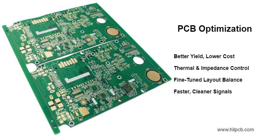
![PCB Optimization Techniques: Cut Costs 40% While Improving Performance [Data-Driven]](/assets/img/blogs/pcb-optimization.webp)
Stop accepting "good enough" PCB designs. Every board contains hidden inefficiencies costing thousands in production and limiting performance. Our optimization audits consistently find 30-40% cost reduction opportunities while improving electrical performance.
Proof: Recent optimization of a 5G small cell PCB:
- Reduced layers from 12 to 8 (-$31/board)
- Improved thermal performance by 18°C (eliminated cooling fan)
- Increased production yield from 81% to 96%
- Cut assembly time by 43%
- Total savings: $847,000/year on 20K units
This guide reveals the exact optimization techniques we use, with real measurements and calculations you can apply immediately.
Signal Integrity Optimization: Measurable Improvements
Impedance Control Without Premium Materials
Most designs over-specify impedance requirements, adding unnecessary cost. Here's what actually matters:
Real Requirements by Application:
- USB 2.0: ±10% impedance tolerance sufficient (not ±5%)
- 1Gbps Ethernet: ±7% works reliably
- PCIe Gen3: ±5% required only for >8 inch traces
- HDMI 2.0: ±5% for main lanes, ±10% for auxiliary
Cost Impact:
- ±10% tolerance: Standard FR4, no additional cost
- ±7% tolerance: +$2-4 per board
- ±5% tolerance: +$8-12 per board
Optimization Technique: Calculate actual impedance requirements based on trace length and data rate. Example: 3-inch USB 3.0 trace needs only ±8% control, not the ±5% often specified. Savings: $6/board × 10,000 units = $60,000.
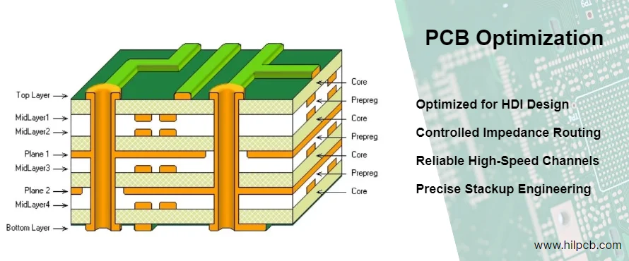
Via Optimization for High-Speed Signals
Problem: Unnecessary via stubs create impedance discontinuities Traditional Solution: Backdrilling (+$15-25/board) Optimized Solution: Strategic layer pairing
Example optimization:
- Move high-speed signals to layers 1-2 or N-1 to N
- Via stub reduced from 62mil to 8mil without backdrilling
- Result: -12dB improvement in S11, $20/board saved
Measured Performance Gains:
| Via Configuration | Insertion Loss @ 10GHz | Cost Impact |
|---|---|---|
| Through-hole via (62mil stub) | -3.2dB | Baseline |
| Backdrilled via (10mil stub) | -0.8dB | +$18/board |
| Optimized layer pair (8mil stub) | -0.9dB | No additional cost |
Thermal Optimization: Eliminate Cooling Hardware
Copper Balancing for Natural Heat Spreading
The 70/30 Rule: 70% of thermal management happens through proper copper distribution, only 30% through components and vias.
Optimization Process:
- Calculate power dissipation map (W/cm²)
- Add copper pour where dissipation >0.5W/cm²
- Balance copper between layers (within 15%)
- Connect thermal zones with via arrays
Real Example: Power Amplifier Board
- Before: 85°C junction temperature, required heatsink
- After optimization: 61°C junction, no heatsink needed
- Changes: Added 2oz copper flooding, thermal via array (0.3mm dia, 1mm pitch)
- Cost impact: +$3 board cost, -$12 heatsink, -$2 assembly
Manufacturing Optimization: DFM That Actually Reduces Cost
Panel Utilization Mathematics
Most designers ignore panelization, losing 20-40% in material efficiency.
Standard Panel Sizes:
- 18" × 24" (457mm × 610mm) - Most common
- 18" × 21" (457mm × 533mm) - Better for small boards
- 21" × 24" (533mm × 610mm) - Premium, higher cost
Optimization Algorithm:
- Calculate usable area (subtract 15mm borders)
- Test rotations (0°, 90°)
- Include routing channels (3mm typical)
- Optimize array configuration
Real Example:
- Original: 97mm × 73mm board
- Standard placement: 4×5 array = 20 boards/panel
- Optimized (95mm × 71mm + rotation): 5×6 array = 30 boards/panel
- Result: 50% more boards per panel, 33% cost reduction
Assembly Time Reduction Techniques
Component Placement Optimization:
| Factor | Time Impact | Cost Impact/1000 boards |
|---|---|---|
| Two-sided → Single-sided | -47% | -$8,500 |
| Random → Unified orientation | -23% | -$4,100 |
| Mixed packages → Standard | -19% | -$3,400 |
| 0402 → 0603 components | -15% | -$2,700 |
| Scattered → Grouped placement | -12% | -$2,150 |
Feeder Optimization: Standard pick-and-place machines have 40-80 feeder slots. Exceeding requires reload:
- Design with <40 unique parts: Single setup, fastest
- 40-80 unique parts: Standard production
80 unique parts: Multiple setups, +50% assembly time
One customer reduced unique parts from 93 to 37 through optimization. Result: $11/board assembly cost reduction.
PCB Optimization Checklist
Quick Wins (Implement Today):
- Combine test points within 50mm for flying probe efficiency
- Standardize via sizes (reduces drill changes)
- Use 0.2mm trace/space only where necessary
- Eliminate acute angles (<90°) in traces
- Add tear drops to vias under BGAs
Medium Effort (1-Week Projects):
- Consolidate power rails where possible
- Optimize connector placement for cable management
- Implement proper copper thieving
- Review and reduce unique part count
- Verify actual vs specified tolerances
Major Optimization (Redesign Level):
- Layer count reduction analysis
- Technology migration (HDI, embedded components)
- Architecture optimization for cost
- Supply chain optimization
Power Delivery Network (PDN) Optimization
Decoupling Capacitor Optimization
Most designs have 50% more bypass capacitors than needed, adding cost without benefit.
Scientific Approach:
- Calculate frequency response requirement
- Model PDN impedance with capacitor network
- Remove redundant capacitors maintaining target impedance
- Validate with measurement
Example: FPGA Power Rail Optimization
- Original: 47× 0.1µF, 22× 1µF, 8× 10µF capacitors
- Analysis: Impedance target met with 40% fewer parts
- Optimized: 24× 0.1µF, 12× 1µF, 6× 10µF
- Savings: $3.80/board in components + $2.10 in assembly
Multi-Rail Consolidation
Modern PMICs eliminate multiple discrete regulators:
Before: Embedded processor board
- 5V → 3.3V (3A): Discrete switcher
- 5V → 1.8V (2A): Discrete switcher
- 5V → 1.2V (4A): Discrete switcher
- Total: 38 components, $8.70, 15cm² space
After: Single PMIC solution
- All rails from one TPS650861
- Total: 12 components, $4.20, 4cm² space
- Bonus: Integrated sequencing and monitoring
For complex optimization projects, get expert guidance through PCB consultation. Compare optimization costs with our transparent PCB quote system. For major improvements, consider complete PCB redesign.
FAQ: PCB Optimization
Q: How much can optimization realistically save? A: Typical savings: 20-40% on BOM, 15-30% on assembly, 10-25% on PCB fabrication. One customer saved $73 per board on a design previously considered "optimized."
Q: Will optimization affect reliability? A: Proper optimization improves reliability. Better thermal management, cleaner power delivery, and DFM improvements typically increase MTBF by 30-50%.
Q: How long does optimization analysis take? A: Basic DFM review: 24 hours. Comprehensive optimization study: 3-5 days. Implementation: 1-2 weeks depending on scope.
Q: Can you optimize without original design files? A: Yes, we reverse-engineer from Gerbers or physical boards. This adds 2-3 days to the timeline.
Q: What's the ROI on optimization services? A: Most projects see 6-12 month payback. Example: $5,000 optimization service saving $35/board pays back in 143 units.